Waveguide manufacturing has a yield problem that does not look like a manufacturing problem. Wafers come out of the coating chamber within drawing tolerance, pass incoming inspection, get diced and assembled, and still produce displays with a faint duplicate of the image offset by a few degrees. The defect is visible to every user, it survives every mechanical adjustment, and it is almost always blamed on assembly alignment. It is usually a coating metric.
Where the ghost comes from
In a geometric waveguide, light enters through an in-coupling element, travels by total internal reflection, and leaves through a series of partially reflective mirrors. Each mirror is designed to send a fraction of the light out of the pupil, typically 15 to 30 percent, with the remainder continuing to the next mirror. The ghost appears when light that has already been out-coupled reflects off the outer surface of the waveguide and re-enters the pupil a second time, at an angle offset by the wedge between the two surfaces.
The cure has three parts, and only one of them is mechanical. The outer surface needs a broadband anti-reflection coating that is actually broadband across the full field angle, not just at the design angle. The two surfaces need a parallelism specification tight enough that the second image lands outside the eye box, usually below 30 arcseconds. And the out-coupling coating needs a reflectance that is uniform enough that the ghost stays below the perceptual threshold instead of brightening wherever the coating runs hot.
Uniformity is the number that kills wafers
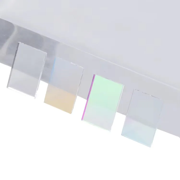
A 300 mm wafer holds dozens of waveguides, and the coating on it is never perfectly uniform. Reflectance may vary by a percent or two across the plate, and centre wavelength by several nanometres. For a single filter in front of a camera, that is unremarkable. For a combiner whose entire function is to distribute light evenly across a pupil, it is a luminance gradient that the eye reads as uneven brightness across the display.
The practical threshold is tight: reflectance uniformity within plus or minus 1.5 percent across the usable area, and centre wavelength within plus or minus 3 nm. A 5 nm shift in a green channel moves colour by roughly 0.004 in u'v', which is at the edge of what a critical user will notice in a side-by-side comparison. Two such shifts on opposite sides of a wafer produce a visible colour split that no calibration file can remove.
Angle, not just wavelength
Geometric combiners are specified at 45 degrees, but the field of view means the actual incidence angle sweeps well beyond that, often 30 to 60 degrees. A dichroic edge designed at 45 degrees shifts toward shorter wavelengths by roughly 0.5 to 1 nm per degree of incidence change at visible wavelengths, and steepens or softens depending on polarisation. Over a 30 degree sweep that is a shift of tens of nanometres, which is why waveguide coatings are designed against an angle-wavelength map rather than a single curve.
This also explains a common field complaint: the image looks correct head-on and shifts colour at the edge of the eye box. The coating is behaving exactly as designed; the design was specified at one angle.
Metrology at wafer scale
Traditional filter metrology measures one point. A waveguide plate needs a map. Nine to twenty-five measurement points across 300 mm, at 1 mm spot size, recording reflection and transmission from 420 to 680 nm, plus a separate angle-resolved scan at three incidence angles. Add a wafer bow measurement, because coating stress on a 0.5 mm substrate curves the plate and changes the effective angle of every subsequent reflection.
Very few optics houses can produce that map, and the ones that can usually built the stage themselves. Buyers who ask for it early discover which suppliers are actually coating waveguides and which are coating filters and calling them waveguides.
The RFQ items that predict yield
Six lines do most of the work. Substrate thickness and tolerance, because 0.5 mm plus or minus 0.02 mm is not the same product as 0.7 mm plus or minus 0.05 mm. Surface parallelism in arcseconds. Reflectance target and uniformity across the pupil, with the measurement grid defined. Centre wavelength and bandwidth per channel. Angle-resolved performance from 30 to 60 degrees. And the metrology report format, agreed before the first wafer is coated.
None of this is exotic. It is simply the difference between buying a coating and buying a yield. On a programme where a single scrapped plate costs more than a month of engineering time, that distinction is the whole commercial case.
Product page: dichroic and beam-splitter filters — specifications, coating options and lead times.