Glass wafers are increasingly the substrate for MEMS, sensors and advanced packaging, often bonded to or interposed with silicon. Cutting them into dies without chipping, heating or cracking the stack is a laser job, and the tolerances are those of a wafer process, not a glazier's. This guide sets out what to specify for laser-cut glass wafers.
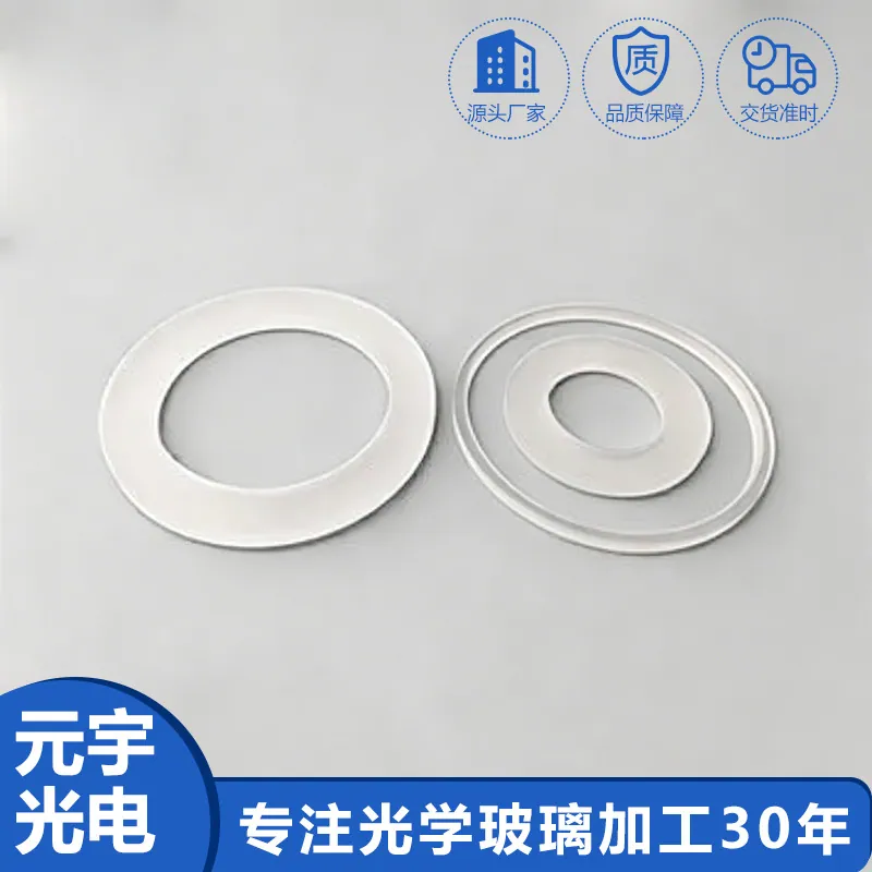
Laser Cutting of Glass in Glass Wafers for MEMS and Sensors
A glass wafer bound for MEMS or a sensor package is a precision substrate: a defined diameter, a tight thickness, and often features such as through-glass vias or a bonded silicon layer. Cutting it into dies must preserve edge quality and flatness without introducing heat or microcracks that later propagate in bonding or reliability testing. Laser cutting is preferred over mechanical dicing here because it can separate brittle glass with a narrow kerf and minimal chipping, and it can be programmed around fragile features rather than forced through them with a blade.
How laser cutting of glass works in practice
The practical tool is an ultrashort-pulse laser, picosecond or femtosecond, whose pulse removes material by ablation faster than heat can spread, leaving a small heat-affected zone. A common route is stealth dicing, where the beam is focused inside the glass to create a modified layer that lets the wafer separate cleanly along a controlled path, often followed by a light expansion or break. The result is an edge with little chipping and no recast bead, which is what a bonded or via'd wafer needs. The process is tuned per thickness and coating stack, because the same parameters do not transfer between a bare wafer and one carrying metal or dielectric.
The tolerances that actually matter
Kerf width and, more importantly, edge chipping below a micrometre class decide whether dies survive handling and bonding. Edge perpendicularity and surface roughness affect how the die seats and seals. Die size and pitch must hold across the wafer so downstream pick-and-place and lithography align. For wafers carrying through-glass vias, the cut must not damage the via walls or the surrounding metallisation, and the edge must remain flat enough that the wafer stays in contact with the chuck and masks through subsequent steps.
Design rules that reduce cost
Uniform thickness and simple, straight or gently curved cut paths are cheapest because they let the beam run at its natural speed without constant acceleration. Avoiding thin bridges and tightly nested features reduces breakage and rework. Tessellation that minimises wasted kerf and a layout that lets cuts run to the wafer edge reduce cycle time. Where a coating is present, designing the cut path to avoid dense metallisation lanes prevents the pulse from splattering metal onto adjacent surfaces, which is a costly cleanup if not planned for.
Coating and deposition considerations
Many of these wafers carry anti-reflection or dielectric coatings, or a bonded stack, and the cut must pass through that stack cleanly without lifting the coating at the edge. The laser parameters are set so the coating is ablated with the glass rather than peeled, because a lifted edge coating is a reliability and leakage path. Where the die face must later be AR-coated or metallised, the cut edge quality determines how cleanly that follows. Through-glass-via wafers add the constraint that the cut and the via process not interact, so the order of operations and the edge proximity to vias are specified together.
Handling, cleaning and packaging
Cut wafers are handled in cassettes and flatpacks under particulate control, because a glass die with a conductive or optical function is easily ruined by a stray particle on its active face. Cleaning after cutting removes ablation debris without attacking the coating or the via metallisation. Packaging holds the wafer flat and supported so the thin glass does not bow or crack in transit, and it is opened in a clean environment so the dies enter the next process without re-cleaning. Traceability to the cut lot lets a downstream yield issue be tied back to the dicing parameters.
Requirements specific to Glass Wafers for MEMS and Sensors
A MEMS or sensor wafer is specified by diameter, thickness and flatness to match the silicon process it joins, and by features such as through-glass vias and bonding layers that the cut must respect. The coefficient of thermal expansion is matched to silicon or the bonded material so the stack does not bow through temperature cycles, and the surface is prepared for the bonding or lithography that follows. The cut is qualified for edge chipping and perpendicularity at the die level, and for via integrity where vias are present, because a cracked via wall or a lifted edge coating fails reliability testing rather than the optical spec. The wafer is delivered in a flat, particulate-controlled package that preserves flatness and supports the next process step directly.
- Ultrashort-pulse cutting for sub-micron edge chipping
- Edge perpendicularity and roughness for sealing and seating
- CTE matched to silicon for bow-free bonding
- Via integrity preserved through the cut
- Flat, particulate-controlled delivery package
Framework references: edge quality and surface figures expressed under ISO 10110 as a framework; the wafer geometry (diameter, thickness, flatness, TTV) follows the semiconductor wafer conventions applicable to the process. Through-glass-via and bonding integrity are qualified per the device reliability specification; confirm the current official text of each standard rather than a single historical value.
Selection data at a glance
| Parameter | Typical capability | Notes |
|---|---|---|
| Cut method | ps / fs ultrashort pulse | low HAZ |
| Edge chipping | sub-micron class | bonding ready |
| Wafer geom | dia, thickness, flatness | silicon match |
| CTE | matched to silicon | no bow |
| Via | intact through cut | reliability |
Frequently asked questions
Why ultrashort pulses instead of a saw?
A blade induces chipping and heat and struggles with coated or via'd wafers. Ultrashort pulses ablate with almost no heat spread, giving clean edges and a narrow kerf that a wafer process can tolerate.
Does the cut damage through-glass vias?
It can, if the path runs too close or the parameters are wrong, which is why via proximity and cut order are specified together. Done correctly the via walls stay intact and the edge coating does not lift.
Why does CTE matter for a glass wafer?
If the glass expands differently from the silicon it is bonded to, the stack bows through temperature cycles and breaks alignment or bonding. Matching CTE keeps the assembly flat across the process window.
Need a quotation for laser cutting of glass?
Send your drawing, target specification or coating requirement and an optical engineer will reply within 24 hours with a price and a lead time.
Request a Quote Email an engineer