Micro-LED and mini-LED mass transfer leans on laser-cut glass carriers and substrates, because the edge quality and absence of micro-cracks decide how cleanly dies release and land. As pitches shrink and panels grow, the cutting process becomes part of the yield equation rather than a separate finishing step. This note tracks the design and sourcing trends optical and process engineers should know before specifying laser-cut glass for display mass transfer.
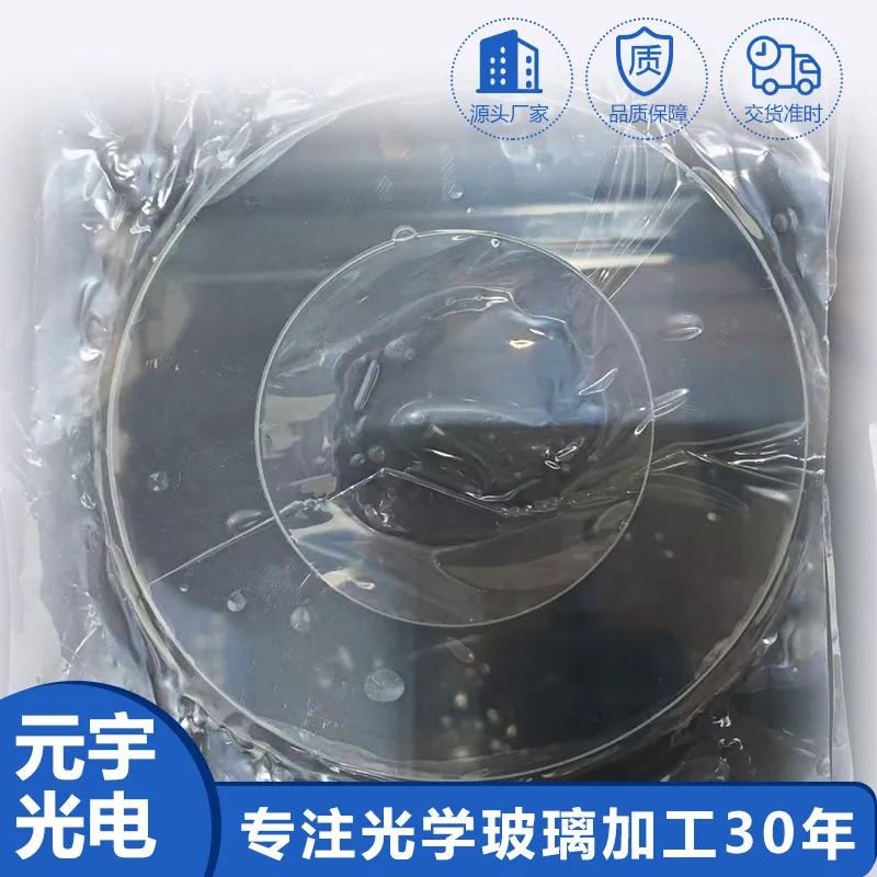
Laser Cutting of Glass in Micro-LED and Mini-LED Mass Transfer
Micro-LED and mini-LED mass transfer leans on laser-cut glass carriers and substrates, because the edge quality and absence of micro-cracks decide how cleanly dies release and land. As pitches shrink and panels grow, the cutting process becomes part of the yield equation rather than a separate finishing step. This note tracks the design and sourcing trends optical and process engineers should know before specifying laser-cut glass for display mass transfer.
What drives cost and lead time
Cost is driven by glass thickness, the cut length per panel and the yield lost to edge defects. Thin glass cuts faster but is harder to handle without breakage, and finer pitch demands tighter edge control that slows the process. Sourcing from a supplier already running the thin-glass format and the laser process in volume shortens lead time more than negotiating the per-panel price, because the bottleneck is process maturity, not material cost.
How laser cutting of glass works in practice
In practice the beam either ablates a kerf or induces a controlled internal modification that the glass then separates along, and the result is judged by edge straightness, chipping and the absence of subsurface cracks. For mass transfer the cut must not leave stress that later propagates during bonding or thermal cycling, so the process window is set by edge integrity rather than by raw cutting speed. The glass is both the carrier being cut and, in some flows, the temporary substrate released by laser lift-off.
Design rules that reduce cost
Keep the glass as close to a standard thin format as the process allows, because custom thickness multiplies handling and yield loss. Design cut paths and die pitch to the laser's proven resolution rather than a theoretical minimum, and specify edge limits only where release or placement demands them. The economical panel is the one whose glass spec was written for the transfer process, not lifted from a maximally tight display catalogue.
Standards, documentation and traceability
For a substrate that becomes part of a display build, edge-quality criteria and lot traceability are part of the specification. Request the measured edge chipping, the subsurface crack depth if characterised, and the flatness or warp of the thin sheet, and keep lot records so a transfer-yield drop can be traced to a cutting batch. A documented, consistent source beats a cheaper unnamed process when the line has to stay qualified.
Requirements specific to Micro-LED and Mini-LED Mass Transfer
Mass-transfer duty makes edge quality a yield parameter, so crack-free, straight cuts and stable thin-glass handling lead the specification. Choose a format the supplier runs in volume, set edge limits to the release and placement need, and keep lot traceability for yield audit. A panel cut to a maximal edge spec but sourced from an immature process will cost more and yield less than a well-controlled standard build.
- Edge quality judged as yield parameter
- Subsurface cracks characterised, not assumed
- Standard thin format to protect yield
- Cut pitch set to proven resolution
- Edge limits only where transfer needs
- Lot traceability kept for yield audit
Framework references: edge quality and dimensional tolerances per ISO 10110; process qualification aligned with the relevant display or semiconductor packaging practice. Environmental declarations such as RoHS are the supplier's to state against the current official text, not to be assumed for a component used in a display build.
Selection data at a glance
| Parameter | Typical capability | Notes |
|---|---|---|
| Thickness | Standard thin | Yield |
| Edge | Crack free | Release |
| Pitch | Proven res. | Process |
| Limits | Transfer need | Cost |
| Trace | Lot kept | Audit |
| Source | Volume mature | Lead |
Frequently asked questions
Why is edge quality a yield issue here and not just cosmetics?
Because the cut edge is where dies release and where stress can propagate during bonding or thermal cycling. A chipped or cracked edge lowers placement yield and can fail later in the field, so the cut is qualified on crack depth and straightness, not on appearance.
Does thinner glass always cut better?
Thinner glass cuts faster but is far easier to break in handling and fixturing, which can cost more in yield loss than the cutting step saves. The economical choice is the thinnest format the line can handle reliably, not the absolute minimum.
What should I trace when transfer yield drops?
Keep lot-level records of edge chipping, subsurface crack depth and sheet flatness from the cutting source, so a yield shift can be correlated to a batch. Without that traceability the failure is a mystery; with it, the responsible process step is obvious.
Need a quotation for laser cutting of glass?
Send your drawing, target specification or coating requirement and an optical engineer will reply within 24 hours with a price and a lead time.
Request a Quote Email an engineer