Requirements in semiconductor and photolithography have been shifting - thinner parts, wider bands, harsher environments - and those shifts change what laser cutting of glass suppliers are being asked to hold. This article reviews where the demand is heading, what it means for specifications, and how to structure sourcing so that a design is not locked to a single process.
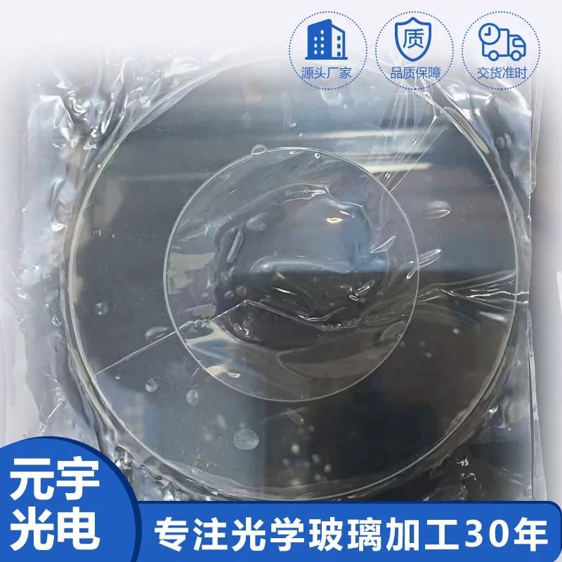
Laser Cutting of Glass in Semiconductor and Photolithography
In semiconductor and photolithography, that translates into a specific set of requirements rather than a general preference for quality. Inside a fab, an optical component is a contamination risk as much as an optical part. Quartz windows, wafers and inspection optics must be made from qualified material with controlled metal content, cleaned to particle specifications, and documented well enough to survive an audit. Deep ultraviolet transmission and homogeneity decide optical performance.
Design rules that reduce cost
Laser cutting rewards drawings that suit the process. Keep cut edges away from optical surfaces, since a cut edge will never have the surface quality of a polished face. Design holes at least one material thickness from the edge and avoid narrow webs that will warp or break during handling. Internal corners should carry radii, because even a laser leaves a stress concentration at a sharp vertex. Where the part will be coated, restrict the coating to the aperture and leave the edge bare. Specify chip size and taper explicitly; if neither is stated, the shop will choose a process that meets the price rather than the application. For Semiconductor and Photolithography, a short note on the drawing about post-cut thermal or mechanical exposure is worth more than any tolerance, because it lets the process be selected correctly the first time.
Standards, documentation and traceability
Laser-cut glass is qualified against the same drawing standards as any optical part, ISO 10110 and its associated imperfection standards, supplemented by specific requirements for edge chip size, roughness and taper. Where the part is used in a safety-relevant system, edge strength testing may be specified. Cleanliness and particle limits arrive from the customer's assembly environment, particularly in semiconductor and medical applications. Environmental compliance is documented through RoHS and REACH declarations. In Semiconductor and Photolithography, the documentation that most often matters is a process record identifying which cutting method was used, because it determines whether the edge can be reworked if the specification changes.
What drives cost and lead time
Laser cutting has essentially no tooling cost and a moderate per-part cost, which makes it ideal for prototypes, low volumes and complex outlines that would otherwise need a mold or a machined profile. The per-part cost scales with the total cut length, the thickness and the number of passes, so a large outline with many holes costs more than a simple rectangle of the same area. Ultrafast processing is slower and more capital-intensive than CO2, so it carries a higher rate per meter cut, offset by the elimination of a finishing step. In Semiconductor and Photolithography, the economic crossover usually appears when the number of parts is large enough that hard tooling would amortise, or when the edge specification is loose enough that thermal cutting plus grinding is cheaper.
How laser cutting of glass works in practice
Laser cutting removes material with light rather than with a wheel, and for glass that changes the economics as well as the quality. There is no hard tooling, so a new outline costs a drawing rather than a mold, and there is no tool wear, so the hundred-thousandth part is cut the same way as the first. Three methods dominate. A CO2 laser heats the glass until it fractures along a controlled path, which is fast and cheap but leaves a heat-affected zone and microscopic cracks. Ultrafast lasers in the picosecond or femtosecond range focus inside the material and create a filament that modifies the glass along a line, after which a small force separates the part - the result is a clean edge with no micro-cracks. Scribe-and-break sits between the two, using a shallow score followed by mechanical separation. In Semiconductor and Photolithography, the choice is usually set by edge quality and by whether the part must survive subsequent thermal or mechanical stress.
Requirements specific to Semiconductor and Photolithography
In semiconductor and photolithography, that translates into a specific set of requirements rather than a general preference for quality. Inside a fab, an optical component is a contamination risk as much as an optical part. Quartz windows, wafers and inspection optics must be made from qualified material with controlled metal content, cleaned to particle specifications, and documented well enough to survive an audit. Deep ultraviolet transmission and homogeneity decide optical performance.
- Deep UV transmission with controlled OH content
- Particle cleanliness measured per unit area
- Homogeneity and low birefringence
- Full material traceability including metal content
SEMI standards for wafer handling and cleanliness, ISO 10110 for optical drawings, and fab-specific material specifications.
Selection data at a glance
| Parameter | Typical capability | Notes |
|---|---|---|
| Cutting methods | CO2 thermal, ultrafast filamentation, scribe and break | Selected by thickness and edge spec |
| Kerf width | 20 - 100 micrometers (ultrafast) | CO2 is wider, water-assisted narrower |
| Edge quality | no micro-cracks with ultrafast, Ra < 1 micrometer | Thermal methods leave a heat-affected zone |
| Thickness range | 0.05-20 mm | Ultrafast preferred below 1 mm |
| Outline tolerance | ±0.05 mm typical, ±0.02 mm on small parts | Complex contours without tooling |
| Edge chips | ≤ 0.02 mm with ultrafast | CO2 needs post-processing |
| Taper | < 5 micrometers per 100 micrometers of depth | Ultrafast, low-taper |
| Set-up cost | none - no hard tooling | Economical from one piece |
| Ideal for | thin glass, tempered glass, complex outlines, wafers | Also drills holes and slots |
Frequently asked questions
Do I need to specify the cutting method?
You should specify the outcome - chip size, taper, edge roughness and post-cut service conditions - and let the process follow from that. Naming a method without stating the requirement often produces an edge that measures correctly and fails in the field.
Does laser cutting leave micro-cracks?
It depends on the process. Ultrafast filamentation cutting produces an edge with no micro-cracks and chips below 0.02 mm. CO2 thermal cutting leaves a heat-affected zone and requires edge grinding or polishing if the part will be stressed.
Can you cut chemically strengthened glass?
Yes, and ultrafast filamentation is the preferred method because it introduces very little heat and preserves the compressive surface layer better than thermal cutting. Cutting before strengthening is the more robust sequence when the geometry allows.
Need a quotation for laser cutting of glass?
Send your drawing, target specification or coating requirement and an optical engineer will reply within 24 hours with a price and a lead time.
Request a Quote Email an engineer