AR Anti-Reflective Glass covers a wider range of options than most drawings imply, and the differences between them decide both performance and price. This article compares the practical choices available for semiconductor and photolithography - substrate, coating process, thickness and tolerance - and shows where each trade-off pays off and where it does not.
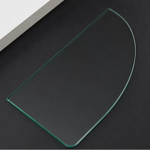
AR Anti-Reflective Glass in Semiconductor and Photolithography
In semiconductor and photolithography, that translates into a specific set of requirements rather than a general preference for quality. Inside a fab, an optical component is a contamination risk as much as an optical part. Quartz windows, wafers and inspection optics must be made from qualified material with controlled metal content, cleaned to particle specifications, and documented well enough to survive an audit. Deep ultraviolet transmission and homogeneity decide optical performance.
How it compares with the alternatives
Alternatives to coating include using a lower-index substrate, laminating a glass to an index-matched adhesive, using an etched or textured anti-glare surface, and simply accepting the reflection. Etched anti-glare glass scatters light rather than suppressing it, which is excellent for readability in bright environments and poor for imaging or transmission. Index matching by lamination works well within a stack but does nothing for the outermost surface. Uncoated glass is often acceptable for a mechanical window and rarely acceptable for anything a user looks through or a sensor looks through. In Semiconductor and Photolithography, the deciding question is whether the system needs more transmitted light or less reflected light - they are related but not identical, and anti-glare treatment solves the second at the cost of the first.
Coating and deposition considerations
AR stacks are built from alternating low-index silica and higher-index oxides such as niobium, tantalum or titanium oxide, deposited in four, six or more layers to flatten the reflectance curve across the band. Broader bands and lower reflectance both require more layers, and more layers mean tighter process control, because each layer contributes to the interference balance. Ion-assisted deposition is preferred for durability: the resulting films are dense, so they resist moisture, resist abrasion and do not shift color when humidity changes. Hydrophobic and oleophobic top layers are frequently added on touch surfaces, and a conductive or anti-static layer helps where dust retention is a problem. For Semiconductor and Photolithography, the deposition process also determines whether the coating can be applied to both faces in one run or needs two passes.
What drives cost and lead time
The cost of an AR coating scales with the number of layers, the area coated and whether one or both faces are treated. A four-layer broadband stack on one face is the economical baseline; pushing average reflectance below 0.2 percent, extending the band, or adding hydrophobic and anti-static functionality each add layers and raise the sensitivity of the run. Coating both faces roughly doubles the process cost but usually costs less than two single-sided parts. Patterned coatings, apertures and masked areas add a lithography or masking step whose cost is dominated by the mask. In Semiconductor and Photolithography, the cheapest improvement is almost always to coat the second surface, since an uncoated rear face often contributes more reflected light than the front coating removes.
Substrate and material selection
The substrate determines what the coating must cope with. B270 and ultra-clear float glass are the standard carriers for displays and instrument windows, offering high transmission at low cost. Borosilicate adds thermal stability, which matters when the glass is tempered, laminated or exposed to heat. Quartz and fused silica extend the band into the ultraviolet and are used where the coating must survive higher energy. Acrylic and polycarbonate are coated when weight matters more than scratch resistance, but they require low-temperature deposition and generally cannot accept the hardest oxide stacks. In Semiconductor and Photolithography, the material also sets the available thickness range, and thin substrates below 1 mm need care both in coating, where warp is a risk, and in assembly, where clamping stress will show up as optical distortion.
Requirements specific to Semiconductor and Photolithography
In semiconductor and photolithography, that translates into a specific set of requirements rather than a general preference for quality. Inside a fab, an optical component is a contamination risk as much as an optical part. Quartz windows, wafers and inspection optics must be made from qualified material with controlled metal content, cleaned to particle specifications, and documented well enough to survive an audit. Deep ultraviolet transmission and homogeneity decide optical performance.
- Deep UV transmission with controlled OH content
- Particle cleanliness measured per unit area
- Homogeneity and low birefringence
- Full material traceability including metal content
SEMI standards for wafer handling and cleanliness, ISO 10110 for optical drawings, and fab-specific material specifications.
Selection data at a glance
| Parameter | Typical value | Notes |
|---|---|---|
| Reflectance per surface | R ≤ 0.5 % average, R ≤ 0.2 % achievable | 420-680 nm |
| Transmission gain | up to 99 % single side, > 99 % both sides | Versus 92 % uncoated B270 |
| Band options | 400-700, 400-1100, 900-1700 nm, dual band | Broadband or tuned |
| Substrate | B270, ultra-clear, borosilicate, quartz, acrylic | 0.5-12 mm |
| Haze | ≤ 0.3 %, typically ≤ 0.1 % | Haze meter |
| Abrasion | pencil hardness 9H, steel wool 0000 pass | Hard oxide stacks |
| Adhesion | tape test 4B or better | Cross-hatch |
| Environmental | 85/85 humidity, salt spray, UV stable | Outdoor grades available |
| Coating pattern | full face, aperture only, or masked | Margin 0.5-1 mm typical |
Frequently asked questions
Do you offer anti-glare as well as anti-reflective treatment?
Yes. Anti-reflective coating maximises transmitted light while anti-glare etching scatters reflected light for readability. Many display products combine a coated front face with an etched surface where the customer wants both.
What reflectance can an AR coating actually reach?
Under 0.5 percent average per surface is routine, and under 0.2 percent is achievable across the visible band with a multilayer stack. Total transmission above 99 percent is possible when both faces are coated.
Should I coat one side or both?
Both, whenever the budget allows. The uncoated rear surface usually reflects as much light as the front coating removes, so leaving it bare gives up most of the benefit and often introduces visible ghosting.
Need a quotation for ar anti-reflective glass?
Send your drawing, target specification or coating requirement and an optical engineer will reply within 24 hours with a price and a lead time.
Request a Quote Email an engineer