Specifying quartz and crystal glass for semiconductor and photolithography is largely a matter of deciding which three numbers actually govern the application and letting the rest follow. This guide walks through the parameters that belong on the drawing, the tolerances that genuinely change the price, and the specification items that are routinely left out and then argued about at first article.
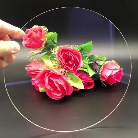
Optical Quartz and Crystal Glass in Semiconductor and Photolithography
In semiconductor and photolithography, that translates into a specific set of requirements rather than a general preference for quality. Inside a fab, an optical component is a contamination risk as much as an optical part. Quartz windows, wafers and inspection optics must be made from qualified material with controlled metal content, cleaned to particle specifications, and documented well enough to survive an audit. Deep ultraviolet transmission and homogeneity decide optical performance.
The tolerances that actually matter
Quartz parts are quoted like other optical elements, but a few tolerances deserve special attention. Flatness and transmitted wavefront are measured at a stated wavelength, and because quartz is stiff and low-expansion, excellent flatness is genuinely achievable rather than nominal. Birefringence is specified in nanometers per centimeter for fused parts and is intrinsic to crystalline material; if the application is polarisation-sensitive, that number belongs on the drawing. For wafers, total thickness variation and warp matter alongside the optical figure, because the part may be processed in a vacuum chuck where flatness is imposed mechanically. Surface quality is quoted in scratch-dig, and edge finish in chip size. In Semiconductor and Photolithography, it is worth stating whether the surface figure must hold at temperature or only at room temperature.
Design rules that reduce cost
Designing with quartz means exploiting its properties without paying for them twice. Use it where the UV transmission, the low expansion or the high damage threshold is actually required, and use ordinary optical glass elsewhere; a hybrid assembly that uses a quartz window and a borosilicate mounting ring has to account for the expansion mismatch, which is significant even though quartz itself moves very little. Keep edges chamfered and avoid clamping directly on an optical face. Avoid specifying both a very thin part and a very tight flatness unless the mounting will support it. For polarisation work, state the axis orientation on the drawing. In Semiconductor and Photolithography, a short design review before the first cut usually removes one of the tight tolerances entirely, which is the cheapest possible redesign.
Coating and deposition considerations
Coating quartz means managing stress and cleanliness. Its low expansion means the substrate will not relieve the stress a dense oxide stack introduces, so on thin parts a coating can visibly bow the window; a balanced design with a stress-compensating layer on the reverse face is sometimes required. Quartz attracts and holds contamination differently from soft glass, so pre-coating cleaning is longer and usually includes a UV-ozone or plasma step. For laser parts, coating absorption and damage threshold dominate the specification, and the coating must be evaluated at the operating wavelength and pulse duration rather than at a convenient broadband average. In Semiconductor and Photolithography, the combination of a hard, low-absorption coating and a chamfered, fine-lapped edge is what makes a quartz window survive both the optical flux and the thermal cycle.
How quartz and crystal glass works in practice
Quartz and crystal glass cover two related but distinct materials. Fused silica is synthetic, amorphous silicon dioxide, made by melting or by chemical vapor deposition, and it is the material of choice whenever a part must work below about 250 nm, survive high laser energy or tolerate rapid temperature change. Crystalline quartz is the natural or grown crystal, valued for its piezoelectric behavior and used in frequency control, polarisation optics and where its specific optical activity matters. Both share a very low coefficient of thermal expansion, about one seventeenth that of soda-lime glass, which is why a quartz window can survive a temperature gradient that would crack ordinary glass. In Semiconductor and Photolithography, that thermal stability combined with deep UV transmission is usually the reason quartz is specified rather than a cheaper optical glass.
Requirements specific to Semiconductor and Photolithography
In semiconductor and photolithography, that translates into a specific set of requirements rather than a general preference for quality. Inside a fab, an optical component is a contamination risk as much as an optical part. Quartz windows, wafers and inspection optics must be made from qualified material with controlled metal content, cleaned to particle specifications, and documented well enough to survive an audit. Deep ultraviolet transmission and homogeneity decide optical performance.
- Deep UV transmission with controlled OH content
- Particle cleanliness measured per unit area
- Homogeneity and low birefringence
- Full material traceability including metal content
SEMI standards for wafer handling and cleanliness, ISO 10110 for optical drawings, and fab-specific material specifications.
Selection data at a glance
| Parameter | Typical value | Notes |
|---|---|---|
| Transmission band | 185-2500 nm (fused silica) | Deep UV to near IR |
| Refractive index | 1.458 (fused silica) | Low and highly uniform |
| CTE | 0.55 × 10⁻⁶ /K | Thermal shock resistant |
| OH content | < 10 ppm low-OH, > 200 ppm high-OH | Selected by UV or IR use |
| Birefringence | < 5 nm/cm (fused) | Crystalline quartz is anisotropic by nature |
| Flatness | λ/4 to λ/10 | Quartz wafers to λ/20 |
| Scratch-dig | 40-20 standard, 20-10 precision | ISO 10110-7 |
| Thickness range | 0.1-30 mm | Wafers from 0.1 mm |
| Edge finish | ground, chamfered or fine-lapped | Chips ≤ 0.05 mm |
Frequently asked questions
Do you supply quartz wafers as well as windows?
Yes, from 0.1 mm upwards, with total thickness variation and warp controlled for vacuum-chuck processing, and with edge profiles selected for automated handling equipment.
When should I choose quartz rather than optical glass?
When the part must transmit below roughly 300 nm, survive a rapid thermal cycle, or withstand high laser energy. For visible-light windows and filters, borosilicate or B270 performs the same function at a fraction of the cost.
What is the difference between low-OH and high-OH fused silica?
Low-OH material has minimal hydroxyl content and transmits further into the infrared. High-OH material contains several hundred parts per million of hydroxyl, which improves deep-UV transmission and resistance to solarisation.
Need a quotation for optical quartz and crystal glass?
Send your drawing, target specification or coating requirement and an optical engineer will reply within 24 hours with a price and a lead time.
Request a Quote Email an engineer