There is always more than one way to solve the optical problem in semiconductor and photolithography, and the options are not equally good at everything. This article compares IR filters against the materials, processes and design approaches it competes with, on the criteria that matter commercially: performance, durability, unit cost and lead time.
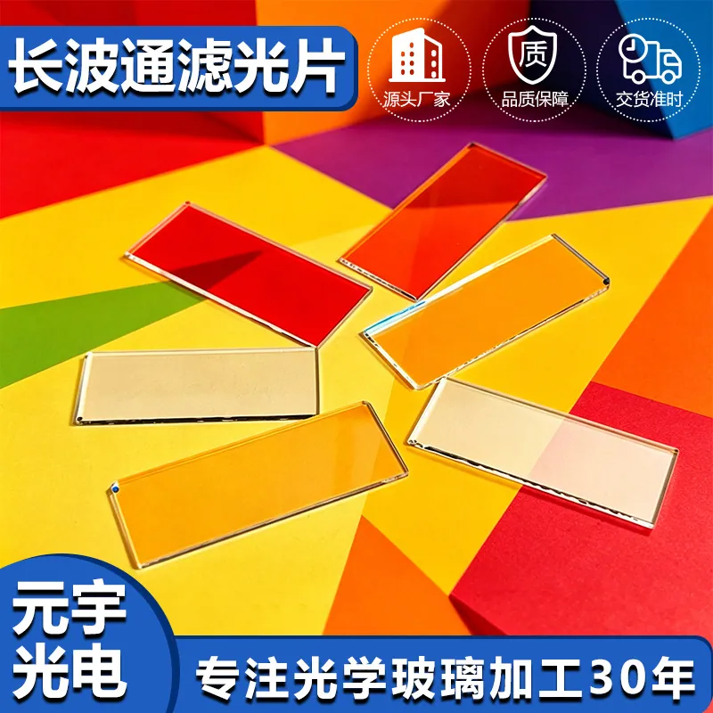
IR Filters in Semiconductor and Photolithography
In semiconductor and photolithography, that translates into a specific set of requirements rather than a general preference for quality. Inside a fab, an optical component is a contamination risk as much as an optical part. Quartz windows, wafers and inspection optics must be made from qualified material with controlled metal content, cleaned to particle specifications, and documented well enough to survive an audit. Deep ultraviolet transmission and homogeneity decide optical performance.
Substrate and material selection
The substrate decides transmission, thickness and durability. B270 and D263T borosilicate are the standard carriers for camera and sensor windows: clear, dimensionally stable, and thin enough to laminate or to fit behind a lens. Absorptive blue glass is used where the NIR must be removed without an angle-dependent coating, and it can also be combined with a dichroic layer to sharpen the edge. Sapphire enters when the window must resist abrasion - handheld devices and outdoor instruments - and its hardness also brings a wider transmission band, out to about 4.5 micrometers. In Semiconductor and Photolithography, the substrate is usually specified together with the cut-on wavelength, because the two interact: a dichroic edge deposited on a substrate with some intrinsic NIR absorption will read further blue than the same stack on clear glass.
What drives cost and lead time
Layer count is the main cost lever. A simple IR-cut stack is a routine chamber run; adding a broadband AR on the second surface, a hydrophobic top layer, or tightening the transition from 30 nm to 10 nm each adds chamber time, increases sensitivity to layer thickness error and reduces yield, so prices rise faster than the layer count suggests. Substrate grade and thickness matter less than expected, except for sapphire, which is materially more expensive in every respect. Size is the second lever: parts that fit comfortably inside the chamber's uniform zone cost far less per unit than parts that must be positioned at the edge, where thickness uniformity degrades. In Semiconductor and Photolithography, the cheapest real saving usually comes from relaxing the angle specification rather than from changing the material.
The tolerances that actually matter
An IR filter is specified by its curve, so the tolerances that matter are spectral. A typical commercial part holds the cut-on wavelength to plus or minus five nanometers and the visible transmission to within a few percent of nominal; precision imaging parts tighten the wavelength to two nanometers and also constrain the slope of the transition. All of these numbers are only meaningful at a stated angle of incidence, and the acceptance angle belongs on the drawing next to the spectral tolerance. Mechanical tolerances follow the mounting: thickness to plus or minus 0.02 mm for a drop-in window, outline to plus or minus 0.05 mm, and a chamfer on every edge. In Semiconductor and Photolithography, the specification most often forgotten is the permitted variation of color across the aperture, which is what a user actually notices when a wide lens produces a green frame edge.
How it compares with the alternatives
The direct alternatives to a coated IR filter are absorptive blue glass, an absorptive dye on a polymer film, and removing the band in software. Absorptive glass has the advantage of being angle-independent and rugged but adds thickness, weight and color cast. Films are cheap and thin, which suits consumer modules, but they degrade under UV and heat and cannot be used at elevated flux. Software correction reduces NIR bleed without any component at all, but it cannot recover information the sensor never resolved separately, and it fails entirely in single-channel or monochrome systems. For instruments, machine vision and outdoor imaging in Semiconductor and Photolithography, a dichroic filter on a thin glass substrate continues to offer the best combination of edge sharpness, transmission and service life.
Requirements specific to Semiconductor and Photolithography
In semiconductor and photolithography, that translates into a specific set of requirements rather than a general preference for quality. Inside a fab, an optical component is a contamination risk as much as an optical part. Quartz windows, wafers and inspection optics must be made from qualified material with controlled metal content, cleaned to particle specifications, and documented well enough to survive an audit. Deep ultraviolet transmission and homogeneity decide optical performance.
- Deep UV transmission with controlled OH content
- Particle cleanliness measured per unit area
- Homogeneity and low birefringence
- Full material traceability including metal content
SEMI standards for wafer handling and cleanliness, ISO 10110 for optical drawings, and fab-specific material specifications.
Selection data at a glance
| Parameter | Typical value | Notes |
|---|---|---|
| IR-cut cut-on | 630-700 nm | Tuned to the sensor response |
| Visible transmission | T ≥ 90 %, R ≤ 1 % | Average 420-620 nm |
| NIR blocking | OD2 - OD4 (1 % - 0.01 %) | 700-1100 nm |
| Edge steepness | 10-30 nm transition | Dichroic designs |
| Angle of incidence | 0-30 deg specified | Passband shifts blue with angle |
| Wavelength tolerance | ± 5 nm standard, ± 2 nm precision | Measured at stated AOI |
| Substrate | B270, D263T, blue glass, sapphire | Absorptive option removes NIR without angle shift |
| Thickness | 0.3-3 mm | 0.55 - 1.1 mm typical for camera windows |
| Environmental | Humidity, salt spray, abrasion tested | MIL-C-48497 / MIL-PRF-13830B |
Frequently asked questions
How tight can the wavelength tolerance be?
Plus or minus five nanometers is routine and plus or minus two nanometers is achievable on precision imaging parts. Tighter than that usually requires sorting parts by measurement, which raises cost sharply.
What cut-on wavelength should I specify?
Most silicon sensors need the cut-on between 650 and 680 nm, before the sensor's NIR response climbs. If the application also has an 850 nm illuminator nearby, tighten the blocking to OD3 and confirm the edge position against the source wavelength.
Why does my image look green at the corners?
That is angular shift. The dichroic edge moves toward shorter wavelengths as the angle of incidence increases, so off-axis rays lose blue light and the frame edges shift color. Solutions are a wider transition, an absorptive element, or moving the filter closer to the stop.
Need a quotation for ir filters?
Send your drawing, target specification or coating requirement and an optical engineer will reply within 24 hours with a price and a lead time.
Request a Quote Email an engineer