Glass microreactors and flow-chemistry chips carry reactive streams through etched channels in thin glass, and laser cutting is how those fragile, feature-dense panels get separated and ported without the chipping and heat stress of a mechanical blade. The trade-offs are between cut quality at the channel edge, the heat the glass sees and the cleanliness the chemistry demands. This note lays out the material, coating and tolerance choices for laser cutting of glass in microreactor and flow-chemistry chips.
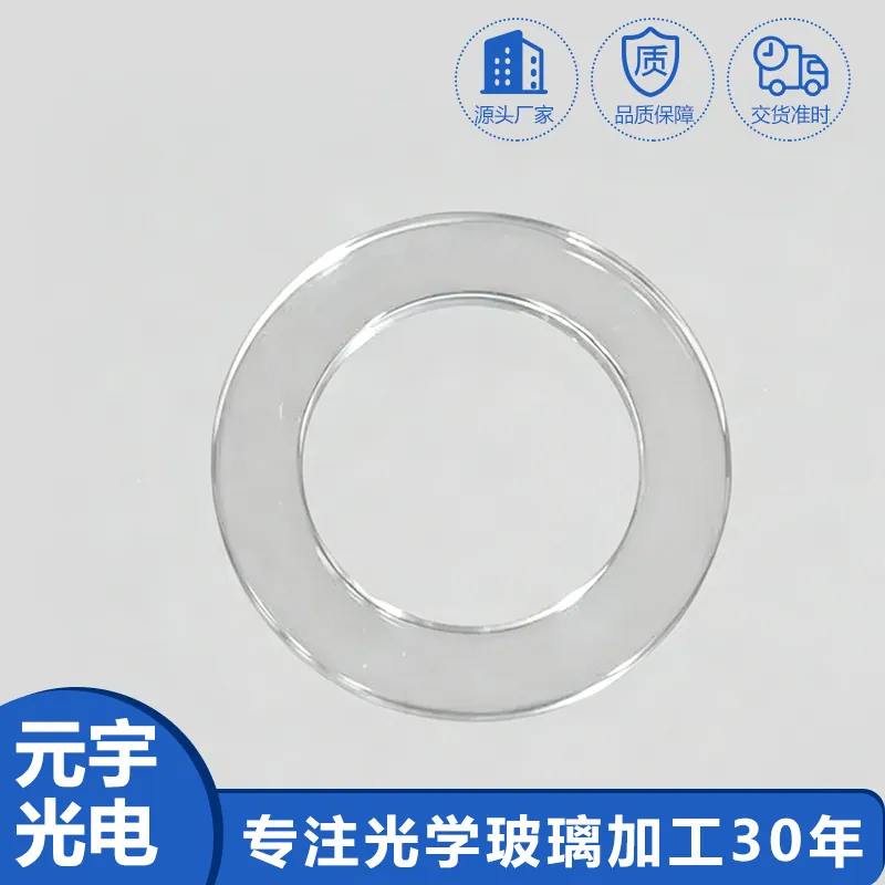
Laser Cutting of Glass in Glass Microreactor and Flow-Chemistry Chips
The laser separates thin glass panels that already carry etched channels and bonded features, so the cut has to be clean at the edge without cracking back into the active area or heating the part enough to disturb the bond. Because the part is chemically active once assembled, the cut edge also has to be free of loose debris and contamination that would foul a reaction. The trade-off is between edge quality, thermal load and the cleanliness the chemistry requires, not speed alone.
Substrate and material selection
Selection starts from the glass type and thickness the chip uses, then picks a laser process matched to that material so the cut is controlled rather than shock-driven. Thin borosilicate and fused-quartz panels cut differently and need different parameters, and the substrate is chosen so the laser wavelength is absorbed at the surface rather than passing through and damaging buried features. The material is matched to the process, because the wrong wavelength or thickness turns a clean kerf into a cracked panel.
How it compares with the alternatives
Laser cutting beats mechanical dicing and scribe-and-break on fragile, feature-dense glass because it avoids the mechanical stress that propagates cracks into channels, but it costs more per cut and needs careful parameter control. Mechanical methods are cheap and fast on robust parts but risk chipping at thin edges; water-jet avoids heat but wets and contaminates a chemistry part. The practical choice is laser where the panel is too fragile or feature-dense for mechanical stress.
Coating and deposition considerations
Where a chip carries a functional coating or a bonded layer, the laser path and energy are tuned so the cut does not burn or lift that layer at the edge, and any debris is removed in a clean post-process. The edge is left smooth enough that the coating or bond remains intact along the channel mouth, and the process is validated against the part's chemistry rather than a generic glass cut. Keep the heat affected zone small, because a disturbed edge is a leak or a fouling site in flow chemistry.
What drives cost and lead time
Cost and lead time are driven by the panel complexity, the yield from edge defects and the cleaning and inspection overhead the chemistry demands. A feature-dense panel with tight edge tolerances leads longer and costs more per cut; a simple outline ships fast. The dominant cost driver is rework from cracked or contaminated edges, so tuning the laser for a clean, cool kerf up front is cheaper than a fast cut that fails inspection.
Handling, cleaning and packaging
Microreactor chips are thin, bonded and chemically sensitive, so handling and cleaning decide both yield and the part's fitness for reaction. Edges are protected through every move, cleaning removes all laser debris without attacking the bond or coating, and the pack keeps the panel flat and contaminant-free to the point of use. Most field failures trace to a contaminated or chipped edge caught at incoming inspection, not to the cut itself.
Requirements specific to Glass Microreactor and Flow-Chemistry Chips
Chip duty makes edge quality, low thermal load and chemical cleanliness the headline trade-offs, so match the laser wavelength and parameters to the glass so the kerf is clean and the buried features survive. Keep the heat-affected zone small so coatings and bonds stay intact at the channel mouth, protect the thin bonded panel through handling, and clean all debris without attacking the chemistry. A cut qualified for the reaction is cheaper than a fast one that fails inspection.
- Wavelength matched to glass
- Clean kerf, no channel cracks
- Small heat-affected zone
- Edge free of debris
- Bond and coating intact
- Clean handling and pack
Framework references: edge-chip, flatness and surface-quality limits per ISO 10110, and coating or bond integrity per the relevant microfluidics or chemistry rule set. Environmental declarations such as RoHS are the supplier's to state against the current official text, not to be assumed for a component used in reactive flow.
Selection data at a glance
| Parameter | Typical capability | Notes |
|---|---|---|
| Material | Matched to laser | No crack |
| Kerf | Clean, cool | Feature |
| HAZ | Small | Bond |
| Coating | Intact at edge | Chemistry |
| Clean | Debris-free | React |
| Handle | Flat, protected | Yield |
Frequently asked questions
Why laser rather than scribe-and-break for these chips?
Because the panels are thin, bonded and feature-dense, and the mechanical stress of scribing propagates cracks back into the etched channels. Laser separates the part without that stress, at the cost of careful parameter control and a clean post-process.
Does the cut heat damage the bonded features?
It can, which is why the wavelength and energy are tuned so the heat-affected zone stays small and away from buried layers. A disturbed edge is a leak or a fouling site in flow chemistry, so the process is validated against the part's actual stack, not a generic glass cut.
What causes the most failures?
Contaminated or chipped edges caught at incoming inspection, which either foul a reaction or leak. Protecting the thin bonded panel through handling and cleaning all laser debris without attacking the bond removes most of that risk.
Need a quotation for laser cutting of glass?
Send your drawing, target specification or coating requirement and an optical engineer will reply within 24 hours with a price and a lead time.
Request a Quote Email an engineer