Thin glass wafers and brittle substrates are increasingly singulated by laser rather than by a mechanical blade, because the laser avoids the chipping and the kerf loss that limit yield on fragile material. The trend is toward processes that leave a clean, strength-preserving edge with no debris on the device side. These notes cover the dicing methods worth specifying and the sourcing rules that keep the edge where the design needs it.
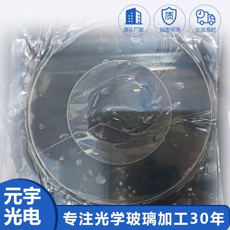
Laser Cutting of Glass in Wafer and Substrate Dicing
In wafer dicing the laser replaces the blade where the material is too thin or too brittle for a wheel, because a beam makes no contact and imposes no cutting force that would chip or crack the edge. The cut either separates the part in one pass or modifies a subsurface layer that a later step cleaves, and the choice sets the edge quality and the debris on the device side. The laser's job is to singulate without weakening the part it is freeing.
What drives cost and lead time
Cost is driven by the process selected and the throughput, because a stealth or a two-step method costs more per cut than a simple through-cut but saves yield that a blade would lose. Lead time tracks the process development on the specific glass thickness and the qualification of the edge, which is slow the first time and fast thereafter. Quoting against a generic cut hides the edge qualification, so the number comes from stating the thickness, the edge spec and the debris rule together.
How laser cutting of glass works in practice
A through-cut scans a focused beam that removes glass along a path, a stealth method modifies a subsurface plane with ultrafast pulses that a later cleave separates, and an edge method shapes the perimeter for strength. In practice the schedule is set by how fast the glass can be cut or modified without leaving a heat-affected zone that weakens the edge, and the edge is measured, not assumed. The process is chosen for the edge it leaves, not just for the line it draws.
Design rules that reduce cost
Cost falls when the edge specification is written to what the device needs rather than to a cosmetic ideal, because an over-tight edge tolerance forces a slower process. Specifying the kerf and the debris rule up front lets the supplier pick the cheapest process that meets them, and standardising thickness and layout avoids custom development. The cheap singulation is the one whose edge spec was written for the part, not borrowed from a display panel.
Standards, documentation and traceability
For diced substrates the records that matter are the edge quality measurement, the debris and contamination check on the device side, and the process parameters tied to a lot, because a weak or dirty edge is a field failure waiting to happen. Dimensional and edge acceptance follows the device's plan, and the process is documented so a yield drop can be traced to a parameter shift. The documentation is what turns a cut into a qualified singulation step.
Requirements specific to Wafer and Substrate Dicing
Dicing duty adds thin, brittle material and a device-side debris rule to the usual constraints, so edge quality and yield lead the process choice. Pick the method by the edge the part needs, specify kerf and debris up front, and require an edge measurement and a lot-traceable process record. Treat the cut as a qualified step with documented parameters, because a diced substrate is judged by the edge it keeps, not by the line it drew.
- Process chosen for the edge needed
- Kerf and debris rule stated
- Edge quality measured, not assumed
- Throughput vs yield balanced
- Lot-traceable process record
- Debris check on device side
Framework references: edge quality and dimension per the device's acceptance plan, with debris and contamination checked on the active side. Environmental declarations such as RoHS are the supplier's to state against the current official text; process qualification follows the equipment rule set applicable to the substrate.
Selection data at a glance
| Parameter | Typical capability | Notes |
|---|---|---|
| Method | Edge it leaves | Yield |
| Kerf | Stated | Layout |
| Debris | Device side | Checked |
| Edge | Measured | Acceptance |
| Process | Lot traced | Yield drop |
| Thickness | Standardised | Dev time |
Frequently asked questions
Why use laser instead of a blade for dicing?
Because thin, brittle glass chips and cracks under a wheel's cutting force, which loses yield and weakens the edge. A laser makes no contact, so it avoids that damage and leaves a cleaner, stronger edge, at the cost of a slower or more developed process that the yield usually pays for.
What does 'stealth dicing' actually do?
It modifies a subsurface plane inside the glass with ultrafast pulses instead of cutting through, and a later step cleaves along that modified layer. The device face stays clean and the edge is strength-preserving, which is why it is chosen where debris on the active side is not allowed.
What specification actually protects yield?
The edge quality and the debris rule on the device side, because a weak or dirty edge is the failure that shows up later. Stating the kerf and the edge spec up front lets the supplier pick the cheapest process that meets them, and measuring the edge turns the cut into a qualified step.
Need a quotation for laser cutting of glass?
Send your drawing, target specification or coating requirement and an optical engineer will reply within 24 hours with a price and a lead time.
Request a Quote Email an engineer