Requirements in semiconductor and photolithography have been shifting - thinner parts, wider bands, harsher environments - and those shifts change what optical glass cold processing suppliers are being asked to hold. This article reviews where the demand is heading, what it means for specifications, and how to structure sourcing so that a design is not locked to a single process.
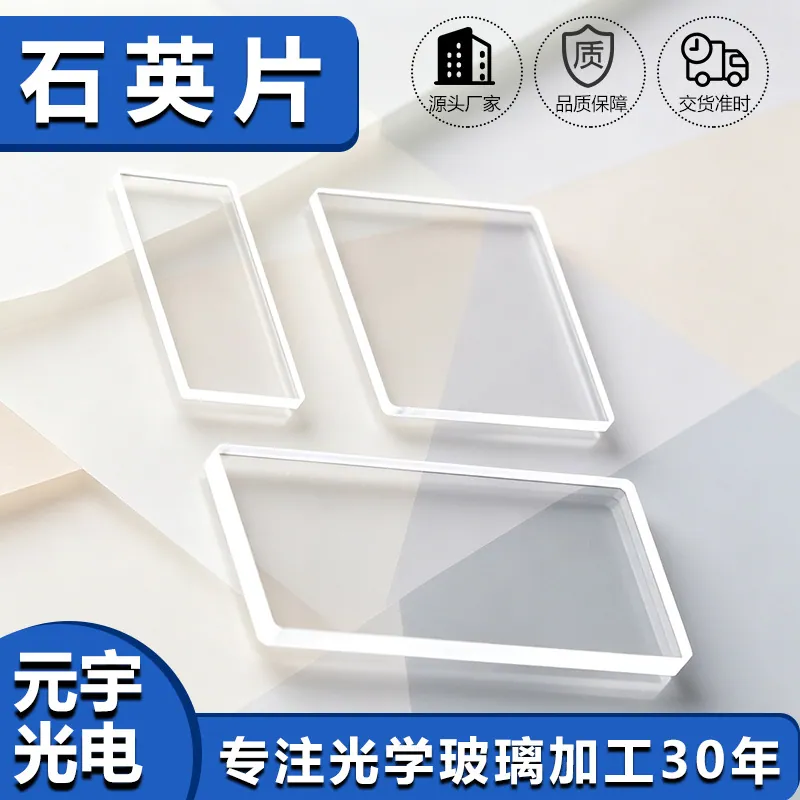
Optical Glass Cold Processing in Semiconductor and Photolithography
In semiconductor and photolithography, that translates into a specific set of requirements rather than a general preference for quality. Inside a fab, an optical component is a contamination risk as much as an optical part. Quartz windows, wafers and inspection optics must be made from qualified material with controlled metal content, cleaned to particle specifications, and documented well enough to survive an audit. Deep ultraviolet transmission and homogeneity decide optical performance.
Design rules that reduce cost
A drawing that respects how glass behaves costs less and ships faster. Keep holes at least one thickness away from an edge and at least two thicknesses apart; glass does not tolerate a thin web between two holes. Replace sharp internal corners with radii of at least 0.5 mm, because a sharp corner is a crack starter. Respect the aspect ratio - a 1 mm hole in 5 mm glass is practical, a 1 mm hole in 20 mm glass is not without ultrasonic or laser drilling. Specify the chamfer rather than leaving it to the shop; an unspecified edge will be whatever the operator considers normal. For Semiconductor and Photolithography, also state the reference surface: which face is the optical face, which datum sets the outline, and whether a coating pattern must register to a machined feature. Half of all first-article queries trace back to an ambiguous datum rather than an impossible tolerance.
Standards, documentation and traceability
Buyers increasingly need a document trail, not just parts. ISO 10110 governs the drawing conventions for optical elements, including surface form, centring and surface imperfections, and ISO 12123 covers raw optical glass specifications. MIL-PRF-13830B remains the common scratch-dig language in North America. Environmental compliance is handled through RoHS and REACH declarations, while automotive and medical programs add IATF 16949, ISO 13485 or ISO 9001 depending on the sector. In Semiconductor and Photolithography, the standards that actually gate a release are usually the customer-specific ones: a cleanliness specification measured in particles per square centimeter, a traceability requirement back to the glass melt, or a first-article inspection report in a defined format. Confirm these before the first part is cut, because retrofitting traceability onto a finished batch is impossible.
What drives cost and lead time
Cost in cold processing is driven by three things: how much material has to be removed, how tight the tolerance is, and how many parts share the setup. Material dominates for sapphire, quartz and large blanks. Tolerance dominates whenever it forces a finishing operation - going from 60-40 to 20-10 scratch-dig roughly doubles polishing labor, and single-point diamond turning is a different cost class entirely. Batch size decides amortisation: a fixture that costs a few hundred dollars is irrelevant across 5,000 parts and decisive across five. The cheapest article to buy is almost never the cheapest to own, though. In Semiconductor and Photolithography, a part that arrives with a consistent edge and a documented coating curve removes an incoming-inspection station, and that saving usually exceeds the price difference between two quotations.
How optical glass cold processing works in practice
Cold processing covers every shaping step that happens at room temperature: cutting the blank from a sheet, generating the outline, grinding the surface to size, lapping and polishing to optical quality, then edging, drilling, chamfering and cleaning. Unlike hot forming, no thermal cycle is applied to the part, so the substrate keeps the optical homogeneity the glass maker certified. For Semiconductor and Photolithography, the practical consequence is that the glass supplier's refractive index, transmission and CTE values survive manufacturing unchanged. Cold processing is normally the only route for parts that must be flat to a fraction of a wavelength, carry a functional coating, or hold a dimensional tolerance tighter than a few hundredths of a millimeter. It is also the route that scales: the same diamond tools and CNC programs that cut one prototype handle a ten-thousand-piece order, which is why most custom optics programs start with a machined sample rather than a molded one.
Requirements specific to Semiconductor and Photolithography
In semiconductor and photolithography, that translates into a specific set of requirements rather than a general preference for quality. Inside a fab, an optical component is a contamination risk as much as an optical part. Quartz windows, wafers and inspection optics must be made from qualified material with controlled metal content, cleaned to particle specifications, and documented well enough to survive an audit. Deep ultraviolet transmission and homogeneity decide optical performance.
- Deep UV transmission with controlled OH content
- Particle cleanliness measured per unit area
- Homogeneity and low birefringence
- Full material traceability including metal content
SEMI standards for wafer handling and cleanliness, ISO 10110 for optical drawings, and fab-specific material specifications.
Selection data at a glance
| Parameter | Typical capability | Notes |
|---|---|---|
| Cutting tolerance | ±0.02 mm standard, ±0.01 mm on CNC | Diamond blade or scribe-and-break |
| Thickness range | 0.05-25 mm | Below 0.3 mm needs carrier fixturing |
| Edge chamfer | 0.1 - 0.3 mm x 45 deg | Edge chips held under 0.05 mm |
| Flatness | λ/4 to λ/10 at 633 nm | Pitch polishing on fused silica |
| Parallelism | ≤ 10 arcsec | Double-side polishing |
| Surface roughness | Ra ≤ 1 nm on polished faces | Ra 0.3 nm achievable |
| Scratch-dig | 40-20 to 60-40 | MIL-PRF-13830B / ISO 10110-7 |
| Minimum hole | 0.5 mm diamond, 0.1 mm ultrasonic or laser | Aspect ratio up to 5:1 |
| Prototype lead time | 5 - 10 working days | Volume runs 15 - 25 days |
Frequently asked questions
What is the fastest route from prototype to production?
Send the drawing and the application, and run the first article as a machined sample rather than a molded or cast part. Machined samples prove the tolerances and the coating at low cost, and the same CNC program then scales into volume production without a redesign.
What tolerances can cold processing realistically hold on glass?
Dimensional tolerances settle around ±0.05 mm as standard and ±0.01 mm with CNC finishing. Optical attributes are quoted separately: flatness to λ/4 or better, parallelism under 10 arcseconds, scratch-dig 40-20 commercially and 20-10 on request. The practical limit is set by how much you are willing to inspect, not by the machine.
Why does my part cost more when I only tighten one dimension?
A single tight dimension usually forces an extra operation and an extra inspection pass, and both are charged regardless of volume. Tightening a thickness from ±0.1 mm to ±0.02 mm can add a lapping stage; tightening surface quality from 60-40 to 20-10 can double polishing time.
Need a quotation for optical glass cold processing?
Send your drawing, target specification or coating requirement and an optical engineer will reply within 24 hours with a price and a lead time.
Request a Quote Email an engineer