Specifying optical glass cold processing for smartphone camera modules is largely a matter of deciding which three numbers actually govern the application and letting the rest follow. This guide walks through the parameters that belong on the drawing, the tolerances that genuinely change the price, and the specification items that are routinely left out and then argued about at first article.
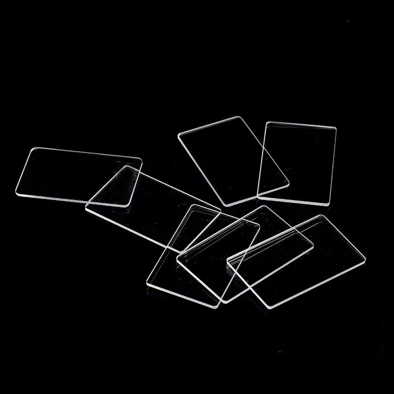
Optical Glass Cold Processing in Smartphone Camera Modules
In smartphone camera modules, that translates into a specific set of requirements rather than a general preference for quality. Phone camera modules are the most space-constrained optical assemblies in mass production. Every component is measured in fractions of a millimeter, the stack is bonded and reflow-adjacent, and the module must survive drop testing, temperature cycling and years of pocket abrasion. Optical requirements center on color fidelity across a wide field of view, low flare from internal reflections, and stable performance after the adhesive cure.
Design rules that reduce cost
A drawing that respects how glass behaves costs less and ships faster. Keep holes at least one thickness away from an edge and at least two thicknesses apart; glass does not tolerate a thin web between two holes. Replace sharp internal corners with radii of at least 0.5 mm, because a sharp corner is a crack starter. Respect the aspect ratio - a 1 mm hole in 5 mm glass is practical, a 1 mm hole in 20 mm glass is not without ultrasonic or laser drilling. Specify the chamfer rather than leaving it to the shop; an unspecified edge will be whatever the operator considers normal. For Smartphone Camera Modules, also state the reference surface: which face is the optical face, which datum sets the outline, and whether a coating pattern must register to a machined feature. Half of all first-article queries trace back to an ambiguous datum rather than an impossible tolerance.
Coating and deposition considerations
Cold processing and coating are one continuous chain, and the interface between them is where most yield is lost. A polished surface must arrive at the chamber with a subsurface-damage layer thin enough that the ion-assisted deposition process can still reach a clean interface; grinding marks that survive polishing show up as scatter, and trapped polishing compound shows up as pinholes after the first warm-up cycle. Chamfers matter more than they look: a sharp edge creates a shadowed, poorly adhered zone and gives the coating a place to lift. For Smartphone Camera Modules, plan the coating before the glass is cut. Coatings that run close to the substrate edge, patterns that must be registered to a machined feature, and selective-area coatings all require locating marks or a mask that has to survive the fabrication steps.
How optical glass cold processing works in practice
Cold processing covers every shaping step that happens at room temperature: cutting the blank from a sheet, generating the outline, grinding the surface to size, lapping and polishing to optical quality, then edging, drilling, chamfering and cleaning. Unlike hot forming, no thermal cycle is applied to the part, so the substrate keeps the optical homogeneity the glass maker certified. For Smartphone Camera Modules, the practical consequence is that the glass supplier's refractive index, transmission and CTE values survive manufacturing unchanged. Cold processing is normally the only route for parts that must be flat to a fraction of a wavelength, carry a functional coating, or hold a dimensional tolerance tighter than a few hundredths of a millimeter. It is also the route that scales: the same diamond tools and CNC programs that cut one prototype handle a ten-thousand-piece order, which is why most custom optics programs start with a machined sample rather than a molded one.
The tolerances that actually matter
Tolerances should be assigned per feature, not globally. Dimensional tolerances of ±0.05 mm are standard and almost free; tightening to ±0.01 mm typically adds a CNC step and a second inspection pass. Optical tolerances are a different currency: flatness is quoted in fringes (one fringe at 633 nm equals 316 nm of sag), surface quality in scratch-dig (40-20 is a normal commercial grade, 20-10 is precision), and parallelism in arcseconds. In Smartphone Camera Modules, the tolerance that usually decides the price is the one nobody writes down - for example the edge chip allowance, the chamfer uniformity, or the difference in thickness across a 100 mm part. Specifying a tolerance that no fixture can hold forces the shop to sort parts instead of making them, and sorting is what turns a two-week lead time into a six-week one.
Handling, cleaning and packaging
Thin and coated glass fails in handling more often than in machining. Below roughly 0.5 mm, parts flex enough that vacuum chucks leave marks and ultrasonic energy can crack edges, so the work is carried on sacrificial plates or wax-mounted to a carrier. After coating, the surface must never touch anything: shippers use a cleanroom-compatible interleaf, edge-protecting trays and, for high-value parts, individual die-cut pockets. Cleaning follows a fixed recipe - alkaline or neutral detergent, cascaded DI rinses, IPA or nitrogen dry - because a change in rinse water quality is enough to leave mineral staining that only appears after the customer's reflow or autoclave cycle. Every handling step in Smartphone Camera Modules should be specified in writing, including the packaging standard, or the same part will arrive in perfect condition once and damaged the next time.
Requirements specific to Smartphone Camera Modules
In smartphone camera modules, that translates into a specific set of requirements rather than a general preference for quality. Phone camera modules are the most space-constrained optical assemblies in mass production. Every component is measured in fractions of a millimeter, the stack is bonded and reflow-adjacent, and the module must survive drop testing, temperature cycling and years of pocket abrasion. Optical requirements center on color fidelity across a wide field of view, low flare from internal reflections, and stable performance after the adhesive cure.
- Thickness typically 0.21 - 0.55 mm
- Transmission above 90 percent in the visible band
- No visible color shading across a wide field of view
- Survives reflow-adjacent temperatures and drop testing
Suppliers usually work to module-maker internal standards covering particle cleanliness, outgassing and bond-line quality, alongside RoHS and REACH declarations.
Selection data at a glance
| Parameter | Typical capability | Notes |
|---|---|---|
| Cutting tolerance | ±0.02 mm standard, ±0.01 mm on CNC | Diamond blade or scribe-and-break |
| Thickness range | 0.05-25 mm | Below 0.3 mm needs carrier fixturing |
| Edge chamfer | 0.1 - 0.3 mm x 45 deg | Edge chips held under 0.05 mm |
| Flatness | λ/4 to λ/10 at 633 nm | Pitch polishing on fused silica |
| Parallelism | ≤ 10 arcsec | Double-side polishing |
| Surface roughness | Ra ≤ 1 nm on polished faces | Ra 0.3 nm achievable |
| Scratch-dig | 40-20 to 60-40 | MIL-PRF-13830B / ISO 10110-7 |
| Minimum hole | 0.5 mm diamond, 0.1 mm ultrasonic or laser | Aspect ratio up to 5:1 |
| Prototype lead time | 5 - 10 working days | Volume runs 15 - 25 days |
Frequently asked questions
What tolerances can cold processing realistically hold on glass?
Dimensional tolerances settle around ±0.05 mm as standard and ±0.01 mm with CNC finishing. Optical attributes are quoted separately: flatness to λ/4 or better, parallelism under 10 arcseconds, scratch-dig 40-20 commercially and 20-10 on request. The practical limit is set by how much you are willing to inspect, not by the machine.
Why does my part cost more when I only tighten one dimension?
A single tight dimension usually forces an extra operation and an extra inspection pass, and both are charged regardless of volume. Tightening a thickness from ±0.1 mm to ±0.02 mm can add a lapping stage; tightening surface quality from 60-40 to 20-10 can double polishing time.
Can you work from a sample instead of a drawing?
Yes, but we will measure it and send the drawing back for approval, because a worn sample may not represent the original design intent. A dimensioned PDF or DXF with a stated datum is always faster and cheaper than reverse engineering.
Need a quotation for optical glass cold processing?
Send your drawing, target specification or coating requirement and an optical engineer will reply within 24 hours with a price and a lead time.
Request a Quote Email an engineer