Optical Glass Cold Processing covers a wider range of options than most drawings imply, and the differences between them decide both performance and price. This article compares the practical choices available for solar and photovoltaic manufacturing - substrate, coating process, thickness and tolerance - and shows where each trade-off pays off and where it does not.
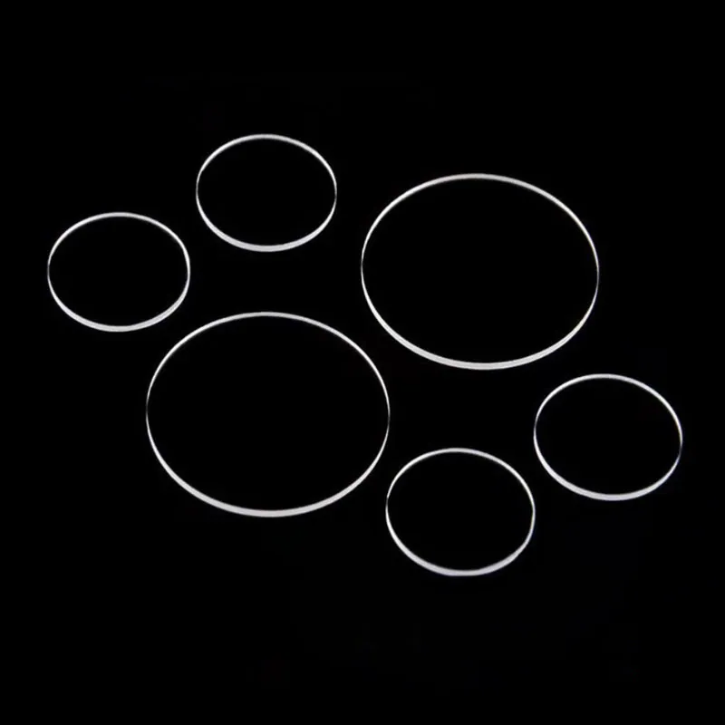
Optical Glass Cold Processing in Solar and Photovoltaic Manufacturing
In solar and photovoltaic manufacturing, that translates into a specific set of requirements rather than a general preference for quality. Solar manufacturing combines very large glass areas with aggressive cost targets and 25-year outdoor exposure. Coatings are used to raise transmission and reduce soiling, while glass is used as tooling and protection in the production equipment itself. Durability under ultraviolet, humidity and thermal cycling is the entry ticket.
What drives cost and lead time
Cost in cold processing is driven by three things: how much material has to be removed, how tight the tolerance is, and how many parts share the setup. Material dominates for sapphire, quartz and large blanks. Tolerance dominates whenever it forces a finishing operation - going from 60-40 to 20-10 scratch-dig roughly doubles polishing labor, and single-point diamond turning is a different cost class entirely. Batch size decides amortisation: a fixture that costs a few hundred dollars is irrelevant across 5,000 parts and decisive across five. The cheapest article to buy is almost never the cheapest to own, though. In Solar and Photovoltaic Manufacturing, a part that arrives with a consistent edge and a documented coating curve removes an incoming-inspection station, and that saving usually exceeds the price difference between two quotations.
Substrate and material selection
Material choice drives nearly every downstream decision. Soda-lime and B270 are cheap and polish quickly, so they suit cover glass and lighting filters where surface quality matters more than index control. Borosilicate 3.3 and Eagle XG bring low thermal expansion, which keeps flatness stable through the coating chamber and through soldering in Solar and Photovoltaic Manufacturing. Fused silica and quartz are chosen when UV transmission, high laser damage threshold or thermal shock resistance is specified; they cost three to eight times more and grind more slowly because of their hardness. Sapphire is the extreme case - nearly scratch-proof and thermally conductive, but it must be machined with diamond tooling and its anisotropy makes polishing direction-sensitive. State the material grade, not just the family: BK7 and B270 are not interchangeable, and a substrate substitution can move a filter's center wavelength by several nanometers.
How it compares with the alternatives
Cold processing competes with three alternatives, and picking the wrong one is expensive. Hot pressing or molding produces aspheres and free-form shapes cheaply at volume, but leaves tool marks that need polishing and cannot hold interferometric flatness without it. Laser cutting and laser ablation skip the tooling and handle complex outlines and holes well, but leave a heat-affected edge and rarely hold tight surface quality on the cut face. Waterjet cutting is fast and thickness-agnostic but leaves a frosted edge that always needs finishing. For most flat optics with a coating and a defined surface figure - the majority of the parts used in Solar and Photovoltaic Manufacturing - conventional cold processing with CNC finishing remains the only route that delivers all three attributes at once: dimensional accuracy, optical surface quality and a coating-ready surface.
Coating and deposition considerations
Cold processing and coating are one continuous chain, and the interface between them is where most yield is lost. A polished surface must arrive at the chamber with a subsurface-damage layer thin enough that the ion-assisted deposition process can still reach a clean interface; grinding marks that survive polishing show up as scatter, and trapped polishing compound shows up as pinholes after the first warm-up cycle. Chamfers matter more than they look: a sharp edge creates a shadowed, poorly adhered zone and gives the coating a place to lift. For Solar and Photovoltaic Manufacturing, plan the coating before the glass is cut. Coatings that run close to the substrate edge, patterns that must be registered to a machined feature, and selective-area coatings all require locating marks or a mask that has to survive the fabrication steps.
Requirements specific to Solar and Photovoltaic Manufacturing
In solar and photovoltaic manufacturing, that translates into a specific set of requirements rather than a general preference for quality. Solar manufacturing combines very large glass areas with aggressive cost targets and 25-year outdoor exposure. Coatings are used to raise transmission and reduce soiling, while glass is used as tooling and protection in the production equipment itself. Durability under ultraviolet, humidity and thermal cycling is the entry ticket.
- Twenty-five year UV and humidity stability
- Very large coated areas with uniform performance
- Hydrophobic or easy-clean surface behavior
- Cost per square meter under pressure
IEC 61215 and IEC 61730 context for module durability, plus RoHS and REACH declarations for the coated glass.
Selection data at a glance
| Parameter | Typical capability | Notes |
|---|---|---|
| Cutting tolerance | ±0.02 mm standard, ±0.01 mm on CNC | Diamond blade or scribe-and-break |
| Thickness range | 0.05-25 mm | Below 0.3 mm needs carrier fixturing |
| Edge chamfer | 0.1 - 0.3 mm x 45 deg | Edge chips held under 0.05 mm |
| Flatness | λ/4 to λ/10 at 633 nm | Pitch polishing on fused silica |
| Parallelism | ≤ 10 arcsec | Double-side polishing |
| Surface roughness | Ra ≤ 1 nm on polished faces | Ra 0.3 nm achievable |
| Scratch-dig | 40-20 to 60-40 | MIL-PRF-13830B / ISO 10110-7 |
| Minimum hole | 0.5 mm diamond, 0.1 mm ultrasonic or laser | Aspect ratio up to 5:1 |
| Prototype lead time | 5 - 10 working days | Volume runs 15 - 25 days |
Frequently asked questions
Why does my part cost more when I only tighten one dimension?
A single tight dimension usually forces an extra operation and an extra inspection pass, and both are charged regardless of volume. Tightening a thickness from ±0.1 mm to ±0.02 mm can add a lapping stage; tightening surface quality from 60-40 to 20-10 can double polishing time.
Can you work from a sample instead of a drawing?
Yes, but we will measure it and send the drawing back for approval, because a worn sample may not represent the original design intent. A dimensioned PDF or DXF with a stated datum is always faster and cheaper than reverse engineering.
How thin can you go before handling becomes the problem?
Around 0.5 mm parts stop behaving like rigid bodies. Below that we mount them on carriers or sacrificial plates, which adds cost but prevents the flexing, chipping and edge damage that otherwise dominate yield.
Need a quotation for optical glass cold processing?
Send your drawing, target specification or coating requirement and an optical engineer will reply within 24 hours with a price and a lead time.
Request a Quote Email an engineer