A part that measures correctly in the lab and fails in service is almost always a qualification gap rather than a manufacturing defect. This article sets out how optical glass cold processing is inspected and qualified for thermal imaging and night vision, which standards apply, which tests reveal real weaknesses, and what documentation should travel with a shipment.
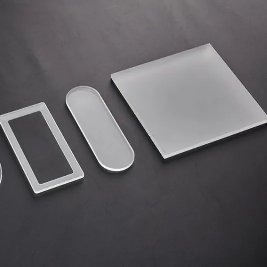
Optical Glass Cold Processing in Thermal Imaging and Night Vision
In thermal imaging and night vision, that translates into a specific set of requirements rather than a general preference for quality. Long-wave infrared systems work in a band where ordinary glass is opaque, which pushes designs toward germanium, silicon, sapphire, zinc selenide and chalcogenide materials. These substrates behave quite differently from visible-light glass: some are soft, some are thermally sensitive, and they require diamond turning or specialised polishing rather than conventional finishing.
Standards, documentation and traceability
Buyers increasingly need a document trail, not just parts. ISO 10110 governs the drawing conventions for optical elements, including surface form, centring and surface imperfections, and ISO 12123 covers raw optical glass specifications. MIL-PRF-13830B remains the common scratch-dig language in North America. Environmental compliance is handled through RoHS and REACH declarations, while automotive and medical programs add IATF 16949, ISO 13485 or ISO 9001 depending on the sector. In Thermal Imaging and Night Vision, the standards that actually gate a release are usually the customer-specific ones: a cleanliness specification measured in particles per square centimeter, a traceability requirement back to the glass melt, or a first-article inspection report in a defined format. Confirm these before the first part is cut, because retrofitting traceability onto a finished batch is impossible.
Common failure modes and how they show up
The recurring failure modes are predictable. Subsurface damage from coarse grinding propagates during final polishing, producing sleeks and latent cracks that only open under thermal cycling. Edge chipping comes from aggressive feed rates or from clamping a part on its optical face. Residual stress from heavy grinding shows up as birefringence, which is fatal in polarisation-sensitive Thermal Imaging and Night Vision optics. Chemical staining appears when a rinse is skipped or when the detergent is not compatible with the substrate. Wedge and thickness variation creep in when a part is lapped on one face only. The remedies are equally predictable: finer grinding steps before polishing, generous chamfers, double-side lapping when parallelism matters, and a cleaning line with verified water quality. When a defect does appear, the useful question is which process step introduced it, and a cross-section or a witness sample usually answers that faster than another round of inspection.
Handling, cleaning and packaging
Thin and coated glass fails in handling more often than in machining. Below roughly 0.5 mm, parts flex enough that vacuum chucks leave marks and ultrasonic energy can crack edges, so the work is carried on sacrificial plates or wax-mounted to a carrier. After coating, the surface must never touch anything: shippers use a cleanroom-compatible interleaf, edge-protecting trays and, for high-value parts, individual die-cut pockets. Cleaning follows a fixed recipe - alkaline or neutral detergent, cascaded DI rinses, IPA or nitrogen dry - because a change in rinse water quality is enough to leave mineral staining that only appears after the customer's reflow or autoclave cycle. Every handling step in Thermal Imaging and Night Vision should be specified in writing, including the packaging standard, or the same part will arrive in perfect condition once and damaged the next time.
Inspection and measurement
Inspection is the difference between a shipment and a rework claim. A credible cold-processing line measures dimensions on a CMM or optical comparator, surface quality against a scratch-dig standard under controlled illumination, flatness on an interferometer, and roughness on a white-light profilometer. Spectrophotometry closes the loop when the part carries a coating. For volume work, the sensible split is 100 % dimensional gauging with statistical process control, plus AQL sampling for cosmetic attributes - inspecting every part interferometrically is possible, but the labor usually costs more than the part. Ask for the inspection record with the shipment, not after it: dimensional reports, coating curves and a traceability sheet with the substrate lot number are what let you release a batch in Thermal Imaging and Night Vision without re-testing it yourself.
Requirements specific to Thermal Imaging and Night Vision
In thermal imaging and night vision, that translates into a specific set of requirements rather than a general preference for quality. Long-wave infrared systems work in a band where ordinary glass is opaque, which pushes designs toward germanium, silicon, sapphire, zinc selenide and chalcogenide materials. These substrates behave quite differently from visible-light glass: some are soft, some are thermally sensitive, and they require diamond turning or specialised polishing rather than conventional finishing.
- Transmission across 8 - 14 micrometers
- Low thermal defocus across the operating range
- Hard carbon or DLC coating for durability
- Athermalised mounting for germanium elements
MIL specifications for IR coatings and surface quality, ISO 10110 drawings adapted for IR materials, and defense-related qualification protocols.
Selection data at a glance
| Parameter | Typical capability | Notes |
|---|---|---|
| Cutting tolerance | ±0.02 mm standard, ±0.01 mm on CNC | Diamond blade or scribe-and-break |
| Thickness range | 0.05-25 mm | Below 0.3 mm needs carrier fixturing |
| Edge chamfer | 0.1 - 0.3 mm x 45 deg | Edge chips held under 0.05 mm |
| Flatness | λ/4 to λ/10 at 633 nm | Pitch polishing on fused silica |
| Parallelism | ≤ 10 arcsec | Double-side polishing |
| Surface roughness | Ra ≤ 1 nm on polished faces | Ra 0.3 nm achievable |
| Scratch-dig | 40-20 to 60-40 | MIL-PRF-13830B / ISO 10110-7 |
| Minimum hole | 0.5 mm diamond, 0.1 mm ultrasonic or laser | Aspect ratio up to 5:1 |
| Prototype lead time | 5 - 10 working days | Volume runs 15 - 25 days |
Frequently asked questions
How thin can you go before handling becomes the problem?
Around 0.5 mm parts stop behaving like rigid bodies. Below that we mount them on carriers or sacrificial plates, which adds cost but prevents the flexing, chipping and edge damage that otherwise dominate yield.
Do you supply material certificates with the parts?
Every shipment carries the substrate lot, a dimensional report and, where relevant, a coating curve. Additional documentation such as RoHS or REACH declarations, first-article inspection reports or full traceability packages can be included when specified at quotation.
What is the fastest route from prototype to production?
Send the drawing and the application, and run the first article as a machined sample rather than a molded or cast part. Machined samples prove the tolerances and the coating at low cost, and the same CNC program then scales into volume production without a redesign.
Need a quotation for optical glass cold processing?
Send your drawing, target specification or coating requirement and an optical engineer will reply within 24 hours with a price and a lead time.
Request a Quote Email an engineer