Photovoltaic manufacturing spent the last decade sampling. A cell line pulled wafers at the start of a shift, imaged them, and extrapolated. That model is disappearing. Cell prices have fallen far enough that a missed defect cluster costs more than the inspection tool, and tandem architectures have made process drift harder to see with the naked eye. The result is 100 percent inspection on the line, at line speed, and a optical train that has to hold its specification across a 230 mm aperture for years.
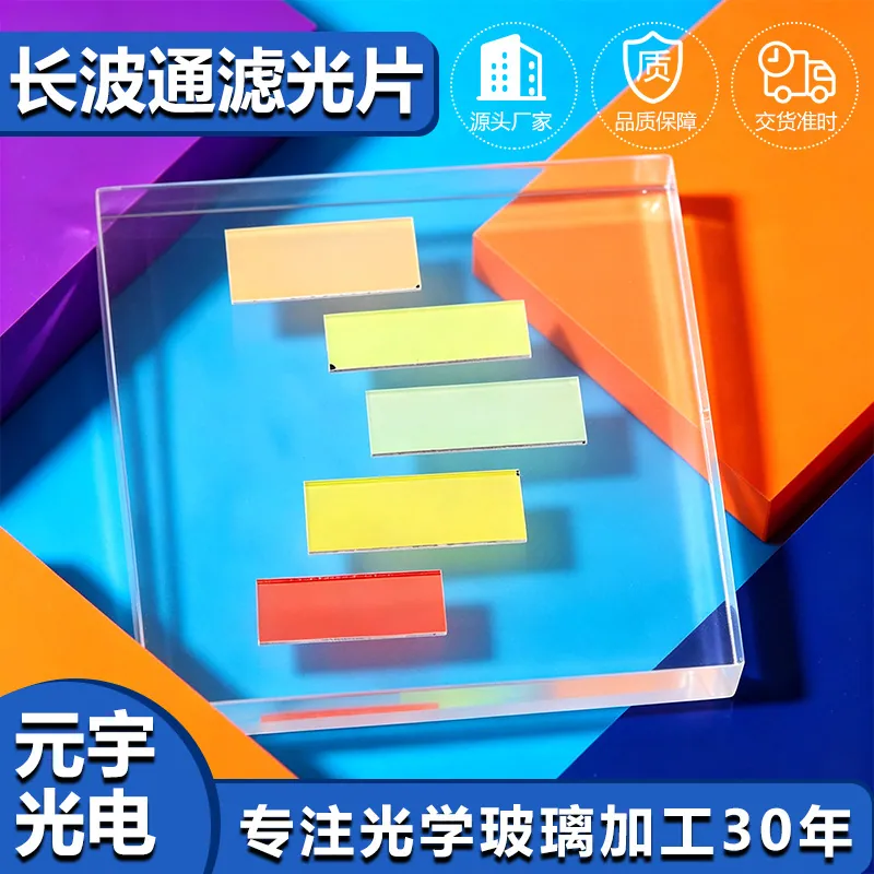
Electroluminescence and photoluminescence are the two workhorses, and they impose different demands on the filters that sit in front of the camera.
Two measurements, two optical problems
Electroluminescence drives the cell forward and images the emission that leaks out of it. For silicon, that emission peaks near 1,150 nm and extends from roughly 900 to 1,250 nm, which is why EL cameras are indium gallium arsenide rather than silicon. The filter's job is to pass that band with high transmission and to reject everything else, including stray illumination from the tool's own handling optics and any ambient light that reaches the enclosure.
Photoluminescence excites with a laser, commonly 808 or 915 nm, and images the resulting emission in the same 1,000 to 1,150 nm window. Here the filter faces a much harder task: the excitation source sits a few tens of nanometres from the signal, and it is many orders of magnitude brighter. A long-pass edge at 950 nm with optical density 6 at the laser line is not a luxury, it is the difference between a lifetime map and a washed-out rectangle.
Tandem cells add a third case. A perovskite layer on silicon emits in two bands, roughly 750 to 800 nm and 1,000 to 1,150 nm, and separating them requires a dichroic splitter rather than a single edge filter. Two cameras, one splitter, and a requirement that both channels stay registered across the aperture as the tool warms up.
The laser line is the whole design
For PL, the blocking specification dominates. Optical density 6 at 915 nm means one part in a million, and that is measured at the design angle, at the design temperature, on the design substrate. Change any of the three and the number moves. A filter quoted at OD 6 at normal incidence will not deliver OD 6 at the 8 degree incidence common in compact inline heads, because the band edge shifts toward shorter wavelengths as the angle increases.
The same angular sensitivity argues for keeping the incidence angle small and fixed. Inline heads that fold the beam to save floor space pay for it in blocking margin.
Uniformity across a 230 mm aperture
A 210 mm wafer needs a filter that is at least 230 mm square, and that is where coating houses separate. Centre-to-edge uniformity of centre wavelength, of edge steepness and of transmission all degrade as the chamber gets larger. A specification of plus or minus 2 nm across the aperture is achievable in a 1.4 m box, but only with planetary rotation that is actually characterised, not assumed.
Why it matters: the edge position sets where the laser line is rejected. If the edge drifts 4 nm from centre to corner, one corner of the image is 4 nm closer to the laser line than the other, and the blocking that was OD 6 in the middle becomes OD 4 at the edge. On a lifetime map that reads as a spatial gradient in carrier lifetime, which is exactly the kind of artefact that sends process engineers chasing a furnace problem that does not exist.
Thermal load and the flatness budget
An inline PL tool may put 1 to 2 kW of 915 nm light through the optical train. A coating with 50 ppm absorption on a 230 mm part still absorbs tens of milliwatts, and more importantly the substrate absorbs in the near infrared if it is not chosen carefully. Fused silica is the default for a reason: low absorption, low expansion, and enough thermal conductivity to spread what it does absorb.
Flatness then becomes a system specification. A 4 mm thick plate that bows by 2 µm under thermal load shifts focus across the field, and on a tool imaging at f/2 that is visible. Three-point mounting with compliant pads, a substrate thickness chosen for stiffness rather than availability, and a flatness callout of lambda/4 over the clear aperture are the usual answers.
Qualifying a supplier for a cell line
Four documents predict whether a filter supplier will survive a production line. A centre-to-edge map of centre wavelength and transmission, measured on the actual part rather than on a coupon. Laser damage data at the working wavelength and power density. A particle and cleanliness specification, because a 50 µm particle in the illumination path prints a permanent dark spot in every image. And evidence that the splitter and the two channel filters for a tandem tool were coated in the same run, so that their edges are matched by construction rather than by luck.
Cell lines do not stop for filter requalification. That single fact explains why the optics conversation in photovoltaic manufacturing has moved from price per part to matched sets, documented uniformity and a supply agreement that covers the second tool as well as the first.
Product page: long-pass and edge filters — specifications, coating options and lead times.