Quantum-computing hardware increasingly relies on ultra-flat, low-loss dielectric carriers and optical interfaces that must hold their geometry from room temperature down to cryogenic operating points, and the cold processing of those glass and glass-ceramic substrates is what delivers the flatness, edge quality and surface finish the system needs. The trend is toward larger, flatter and cleaner substrates with tighter total thickness variation, because any warp or particulate at the carrier level couples into optical and thermal noise at the qubit. These notes track what is changing in how shops process glass for quantum carriers and what to ask a supplier before ordering.
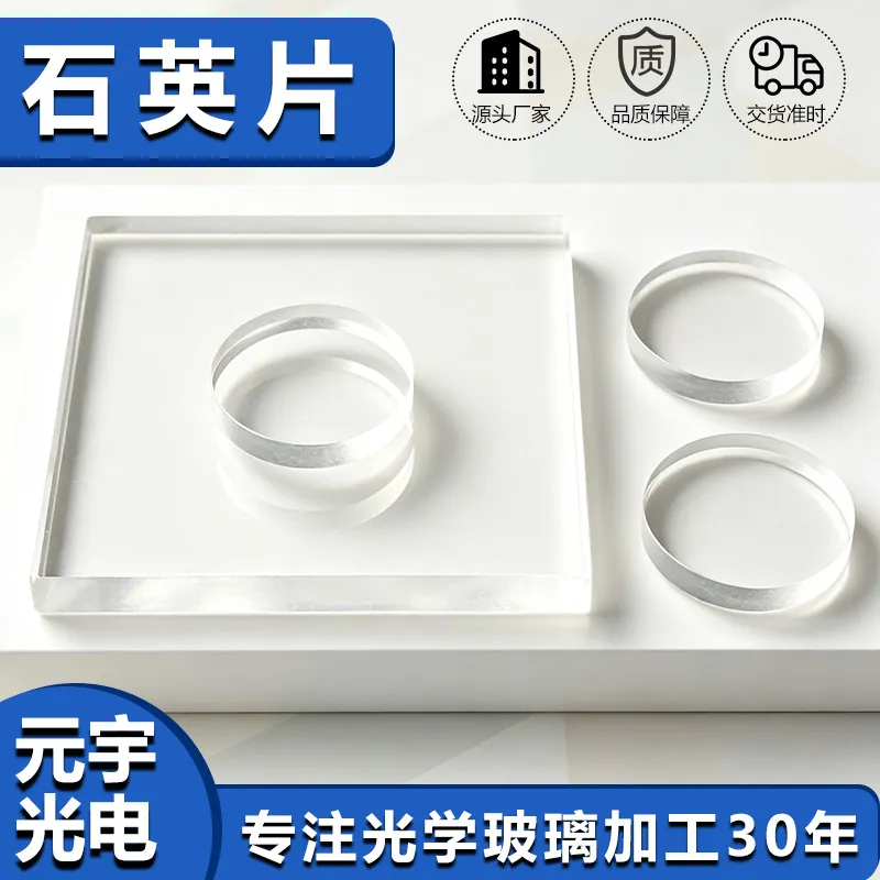
Optical Glass Cold Processing in Quantum-Computing Substrates
Quantum-computing hardware increasingly relies on ultra-flat, low-loss dielectric carriers and optical interfaces that must hold their geometry from room temperature down to cryogenic operating points, and the cold processing of those glass and glass-ceramic substrates is what delivers the flatness, edge quality and surface finish the system needs. The trend is toward larger, flatter and cleaner substrates with tighter total thickness variation, because any warp or particulate at the carrier level couples into optical and thermal noise at the qubit. These notes track what is changing in how shops process glass for quantum carriers and what to ask a supplier before ordering.
Standards, documentation and traceability
Quantum programs expect full material certification, batch traceability and documented process control, because a substrate that cannot be traced to its melt and process is a risk to a multi-month cool-down. Specify the material certificate, the inspection record and the cleanliness class, and keep the documentation chain simple enough to survive an audit. The cost of poor traceability is a scrapped cryogenic run, not a rejected lot.
What drives cost and lead time
Cost is driven by the blank material, the amount of stock removal, and the flatness and surface-finish targets, all of which scale with substrate size. Lead time is dominated by the grinding and polishing loops needed to hit nanometre-class flatness and by any custom fixturing for an unusual shape. Standard round or square blanks from a known glass-ceramic are far faster than a one-off form, so design within the supplier’s standard catalog where the physics allows.
How optical glass cold processing works in practice
The part moves from shaping and edge grinding to deterministic or pitch polishing, with flatness held by controlled removal and by minimising stress from clamping and temperature. Cryogenic-relevant substrates are handled to avoid induced distortion, and the final figure is verified at the temperature the part will actually be used where that matters. In practice the shop that wins is the one that controls thermal and mechanical stress through every step, not the one that simply polishes longer.
Design rules that reduce cost
Cost drops when the flatness and surface-finish targets are set to the qubit carrier’s real needs rather than to a best-available number, and when total thickness variation is held only where stacking demands it. Choose a material the shop processes routinely, keep the aspect ratio friendly to fixturing, and avoid cosmetic specs that force extra polishing. The cheap substrate is the one whose tolerance budget was written for the cryostat, not copied from a metrology catalogue.
The tolerances that actually matter
For a quantum carrier the figure, flatness and total thickness variation control stray optical and thermal paths, and edge quality controls where the part seats and how it is handled. Surface roughness matters where scattering couples into the optical train; for a purely mechanical carrier it can be relaxed. The tolerances that matter are the ones that move the qubit environment, not the generic catalogue limits.
Requirements specific to Cold Processing for Quantum-Computing Glass Substrates
Quantum-carrier duty pushes cold processing to cryogenic-relevant flatness and cleanliness, so figure stability and traceability lead the specification. Pick a glass or glass-ceramic the shop processes routinely, set flatness and total thickness variation to the stack’s real needs, and demand batch certification and a clean handling chain. Qualify the part against the cryostat’s geometry and cleanliness class rather than a generic surface number.
- Flatness and TTV set to the cryostat stack, not a best-available figure
- Material from a routine shop process (glass-ceramic preferred for stability)
- Full melt-to-part traceability and process documentation
- Controlled clamping and thermal stress through every step
- Cleanliness class matched to the qubit environment
- Standard blank shape to avoid custom fixturing lead time
Framework references: surface form, flatness, scratch-dig and edge quality per ISO 10110, and dimensional and cleanliness requirements per the relevant cryogenic or equipment rule set. Environmental declarations such as RoHS are the supplier’s to state against the current official text, not to be assumed for a component used in quantum hardware.
Selection data at a glance
| Parameter | Typical capability | Notes |
|---|---|---|
| Driver | What to specify | Why |
| Figure | Flatness to stack | Optical/thermal noise |
| Material | Routine glass-ceramic | Stable at cryo |
| Trace | Melt + process cert | Audit risk |
| Clean | Class to qubit | Particulate noise |
| Shape | Standard blank | Lead time |
Frequently asked questions
Why is traceability more important than for a normal optic?
Because a quantum carrier that fails at cryogenic temperature can scrap a multi-month cool-down and an expensive package. A substrate traced to its melt and process lets the program isolate the cause and avoid repeating it; an untraceable part is simply a risk no one can manage.
Should I specify the best flatness the shop can hold?
Only if the stack needs it. Flatness and total thickness variation scale cost and lead time sharply, so set them to what the qubit environment actually tolerates. Over-specifying buys polishing loops you do not need and a longer schedule for no physical benefit.
Is a glass-ceramic worth the extra cost over standard glass?
Where dimensional stability across the room-to-cryogenic temperature swing is the constraint, a glass-ceramic’s lower thermal expansion and better figure retention usually pay for themselves by avoiding field failures. For a purely room-temperature interface, standard glass may be enough.
Need a quotation for optical glass cold processing?
Send your drawing, target specification or coating requirement and an optical engineer will reply within 24 hours with a price and a lead time.
Request a Quote Email an engineer