Two quotations for the same coated color filter glass part in semiconductor and photolithography can differ by a factor of three, and the reason is rarely the material. This article breaks down the real cost drivers - tolerance, finishing operations, inspection level and batch size - and shows which specification changes save money and which only look as though they should.
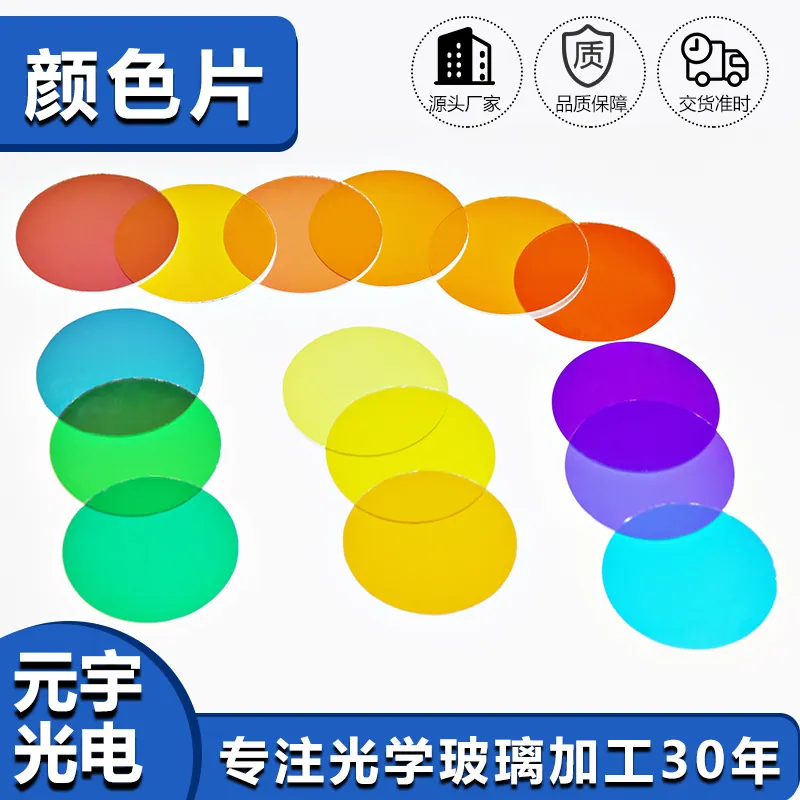
Coated Color Filters in Semiconductor and Photolithography
In semiconductor and photolithography, that translates into a specific set of requirements rather than a general preference for quality. Inside a fab, an optical component is a contamination risk as much as an optical part. Quartz windows, wafers and inspection optics must be made from qualified material with controlled metal content, cleaned to particle specifications, and documented well enough to survive an audit. Deep ultraviolet transmission and homogeneity decide optical performance.
Substrate and material selection
The substrate sets the ceiling on what the coating can survive. B270 and ultra-clear float glass are the workhorses for moderate flux and offer the best price-to-clarity ratio. When the part sits close to a lamp, borosilicate or a specifically heat-resistant glass is used because it tolerates the thermal gradient without cracking; low-expansion substrates such as fused silica or Eagle XG go further and hold their figure through repeated thermal cycling. Thickness matters as much as grade: a 0.5 mm plate heats and cools faster than a 3 mm plate, so thinner is safer under flash or shutter conditions, but more fragile during assembly. For Semiconductor and Photolithography the usual failure is not a material that is too weak, it is a material that was never specified, so the shop defaults to soda-lime and the first high-flux test cracks the plate.
Handling, cleaning and packaging
Coated color plates are handled by the edge, never by the face, and the edge is usually chamfered for exactly that reason. A fingerprint on a dichroic surface is not a cosmetic issue: skin oils etch the outer layer over time and leave a permanent transmission dip. Cleaning uses neutral detergent, cascaded DI rinses and a nitrogen dry, never a dry wipe on a hard oxide stack. Storage and shipping use interleaved, particle-free separators so that two coated faces never touch. For high-value patterned parts going into Semiconductor and Photolithography, individual pockets with a printed label are worth the packaging cost, because a mixed batch of colored plates that has to be re-identified by measuring each one costs far more than the trays.
The tolerances that actually matter
Color work has two tolerance systems that must be quoted together. The spectral tolerance defines how far the transition or the dominant wavelength may sit from nominal - typically ±5 nm for a color chip and ±2 nm for an interference edge used in a measurement path. The geometric tolerance defines where the color sits on the plate, which matters for gobos, patterned filters and multi-zone parts. Add a photometric tolerance for transmission: a filter quoted at 90 % transmission that ships at 82 % is a different color to the eye. In Semiconductor and Photolithography, also fix the angle of incidence at which the numbers are valid, because a coating designed for 0 degrees and measured at 15 degrees will read several nanometers short of nominal and the customer will call it off-spec even though nothing is wrong.
What drives cost and lead time
The price of a coated color filter is mostly a function of the number of layers, the size of the substrate and the yield of the coating run. A 20-layer color coating is routine; a 60-layer edge filter with a 2 nm transition costs several times more because the chamber time and the sensitivity to thickness error both rise sharply. Patterned parts add a lithography or screen-printing step whose cost is dominated by the mask or screen, so the first piece is expensive and the hundredth is not. Substrate grade and thickness contribute less than most buyers expect; the real cost jumps come from tight spectral tolerances, from parts larger than the chamber's uniform zone, and from low volumes that force a chamber to be run for a handful of plates. Consolidating colors that can share one run is the single most effective cost reduction in Semiconductor and Photolithography.
Requirements specific to Semiconductor and Photolithography
In semiconductor and photolithography, that translates into a specific set of requirements rather than a general preference for quality. Inside a fab, an optical component is a contamination risk as much as an optical part. Quartz windows, wafers and inspection optics must be made from qualified material with controlled metal content, cleaned to particle specifications, and documented well enough to survive an audit. Deep ultraviolet transmission and homogeneity decide optical performance.
- Deep UV transmission with controlled OH content
- Particle cleanliness measured per unit area
- Homogeneity and low birefringence
- Full material traceability including metal content
SEMI standards for wafer handling and cleanliness, ISO 10110 for optical drawings, and fab-specific material specifications.
Selection data at a glance
| Parameter | Typical value | Notes |
|---|---|---|
| Dominant wavelength | 450-660 nm, custom to ±5 nm | Per color chip |
| Transmission in band | >= 85 % (T>= 90 % on tuned designs) | At normal incidence |
| Out-of-band blocking | OD2 - OD4 | Visible to NIR |
| Coating type | IAD multilayer hard oxide | Color-by-interference |
| Substrate | B270, borosilicate, ultra-clear, quartz | Heat-resistant grades for high flux |
| Thickness | 0.3-3 mm | 1.1 mm typical for gobos |
| Size tolerance | ±0.1 mm, ±0.05 mm on request | Round, square, custom outline |
| Pattern tolerance | ±0.05 mm registration | Screen print, lithography or mask |
| Operating temperature | up to 400 °C substrate dependent | Thermal shock is the real limit |
Frequently asked questions
Can I combine several colors on one plate?
That is one of the advantages of coating rather than dyeing: a single plate can carry separate coated zones, a patterned logo and an uncoated margin for mounting, all in one coating run. Each zone is designed with its own stack.
How much does a coated color filter shift with angle?
A typical visible-band stack shifts toward shorter wavelengths by roughly 1 % of the wavelength for every 10 degrees of incidence. A design specified for 0 degrees and used in a 30 degree cone will therefore read noticeably bluer than the nominal curve, which is why the acceptance angle belongs on the drawing.
Can you print a logo or pattern in a specific color?
Yes. Patterns are produced by masking or lithography before coating, or by screen printing a patterned layer, with registration typically held to ±0.05 mm. Keep features at least 0.3 mm from the edge and provide artwork as vector data.
Need a quotation for coated color filters?
Send your drawing, target specification or coating requirement and an optical engineer will reply within 24 hours with a price and a lead time.
Request a Quote Email an engineer